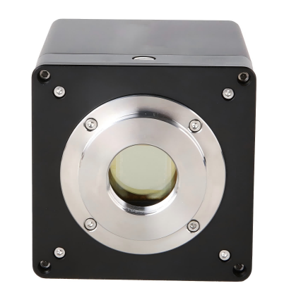

A semiconductor inspection equipment manufacturer needed a camera capable of capturing micro-defects in the EUV spectrum. Attostek customized a high-resolution EUV camera and integrated a dedicated objective lens system, enabling sub-micron defect detection with high precision, contributing to a 20% increase in the client's equipment throughput.
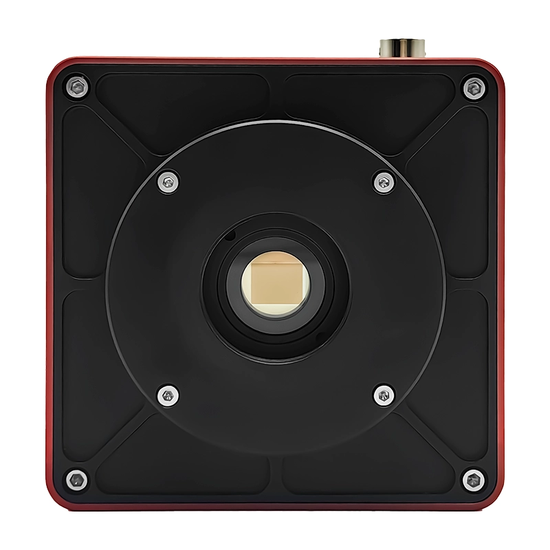
A semiconductor inspection equipment manufacturer needed a camera capable of capturing micro-defects in the EUV spectrum. Attostek customized a high-resolution EUV camera and integrated a dedicated objective lens system, enabling sub-micron defect detection with high precision, contributing to a 20% increase in the client's equipment throughput.
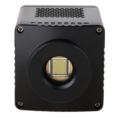
A semiconductor inspection equipment manufacturer needed a camera capable of capturing micro-defects in the EUV spectrum. Attostek customized a high-resolution EUV camera and integrated a dedicated objective lens system, enabling sub-micron defect detection with high precision, contributing to a 20% increase in the client's equipment throughput.
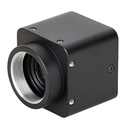
A semiconductor inspection equipment manufacturer needed a camera capable of capturing micro-defects in the EUV spectrum. Attostek customized a high-resolution EUV camera and integrated a dedicated objective lens system, enabling sub-micron defect detection with high precision, contributing to a 20% increase in the client's equipment throughput.
A semiconductor inspection equipment manufacturer needed a camera capable of capturing micro-defects in the EUV spectrum. Attostek customized a high-resolution EUV camera and integrated a dedicated objective lens system, enabling sub-micron defect detection with high precision, contributing to a 20% increase in the client's equipment throughput.