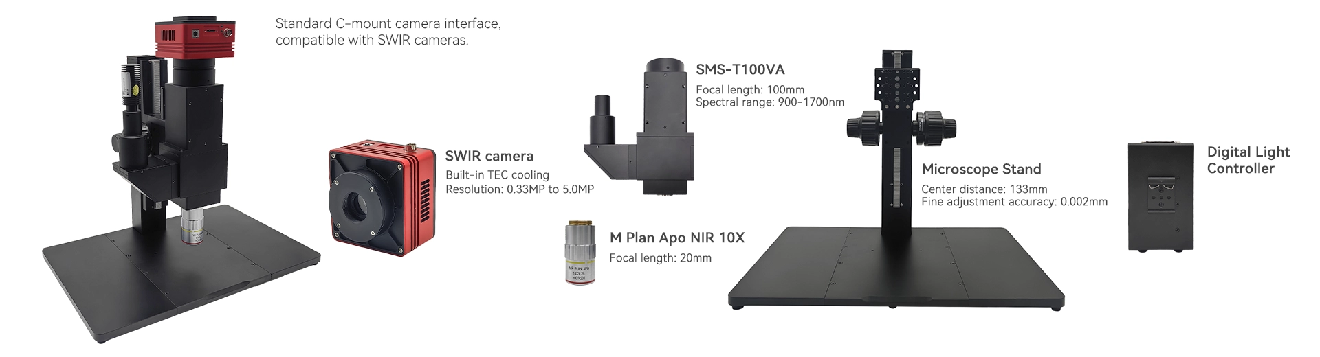
The SMS Series SWIR modular microscopic system extends imaging from the visible spectrum to the 900–1700 nm short-wave infrared (SWIR) band. Featuring standard glass optics and high-sensitivity InGaAs imaging modules, the system ensures compatibility with conventional microscope platforms while enabling penetration inspection of silicon-based materials. Equipped with a standard C‑mount interface, the system is fully compatible with a wide range of SWIR cameras.
| Features |
| SWIR imaging range from 900-1700 nm |
| Dedicated M Plan Apo NIR series objectives (5X to 20X HR) |
| SWIR camera options (0.33M to 5.0M) with built-in TEC cooling |
| Standard C‑mount interface for easy SWIR camera integration |
| Coaxial Kohler illumination with 1200/1300/1400/1550 nm LEDs |
| Precision CNC structure with anti‑vibration design |
| Modular illumination, imaging, and mechanical architecture |
Designed for next-generation material characterization and electronic testing, Attostek’s SWIR Modular Microscopic System delivers exceptional precision and clarity.
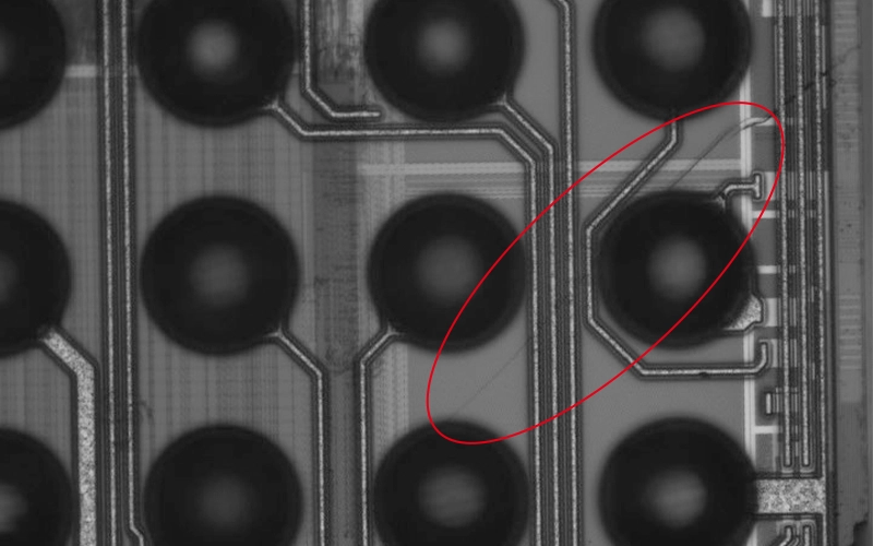
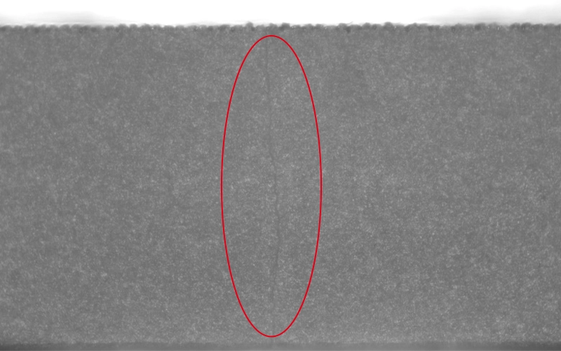
In semiconductor inspection, it reveals subsurface defects, microcracks, hidden chip fractures and soldering defects in silicon wafers and integrated circuits that conventional systems cannot easily detect.
For material science research, it identifies invisible cracks and structural flaws in ceramics, composites and high-performance materials.
In industrial non-destructive testing, it performs non-invasive subsurface component analysis without disassembly, accurately inspecting internal defects in silicon-based materials and ceramic parts.
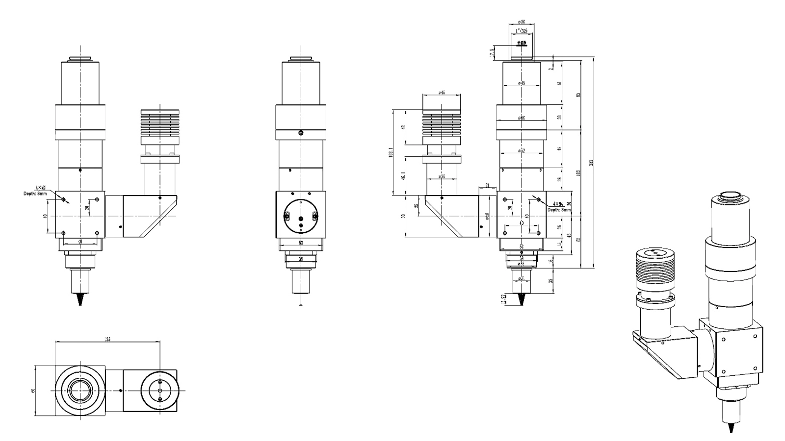
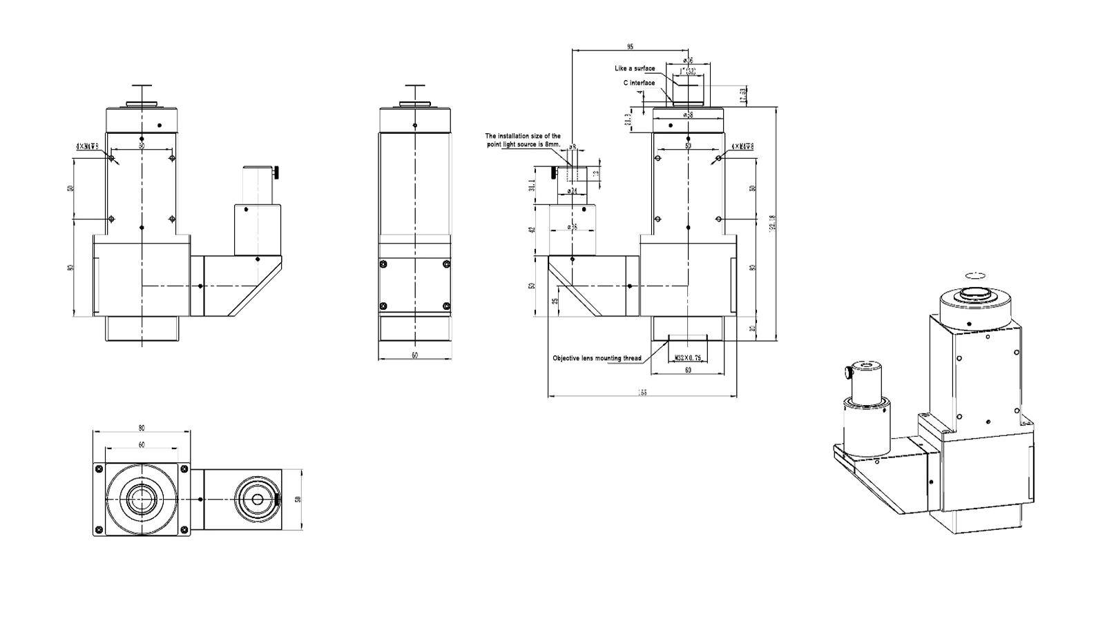
| SMS-T180VA | SMS-T090VA | SMS-T100VA | |
| Objective Support | Support infinity SWIR microscope objectives | Support high NA infinity SWIR microscope objectives | |
| Tube Lens Focal Length | 180mm | 90mm | 100mm |
| Imaging Path Image Plane Size | 24mm (using 180mm focal length tube lens) | 33mm (using 200mm focal length tube lens) | |
| Imaging Path Spectral Range | 900-1700nm | ||
| Camera Mount | C-Mount | ||
| Illumination Method | Coaxial Kohler Lighting | ||
| Illumination Source | 1550/1400/1300/1200nm LED light source | ||
| Item Name | Magnification | Numerical Aperture | Working Distance | Focal Length | Resolution | Depth of Field | FN | Weight |
| M Plan Apo NIR 5X | 5X | 0.14 | 37.5 mm | 40 mm | 2.0 μm | 14 μm | 24 mm | 220 g |
| M Plan Apo NIR 10X | 10X | 0.26 | 30.5 mm | 20 mm | 1.1 μm | 4.1 μm | 24 mm | 250 g |
| M Plan Apo NIR 20X | 20X | 0.4 | 20 mm | 10 mm | 0.7 μm | 1.7 μm | 24 mm | 300 g |
| Model | SWIR051AU | SWIR0503AU | SWIR035AU | SWIR033AU |
| Sensor Model | Sony IMX990 | Sony IMX991 | Sony IMX992 | Sony IMX993 |
| Sensor Size | 1/2″ | 1/1.4″ | 1/1.8″ | |
| Pixel Size | 5μm×5μm | 3.45μm×3.45μm | ||
| resolution | 1.3MP | 0.33MP | 5.0MP | 3.0MP |
| FPS | 392fps | 753fps | 135.7fps | 176fps |
| Data Interface | USB3.0 | |||
| Exposure Time | 15us-60s | |||
| Dimension | 80mm×80mm×45.5mm | |||
| TEC | Built-in TEC | |||
The main advantages include three key aspects:
The SMS series provides multiple tube lens configurations to match different SWIR microscope objectives and image plane requirements. All solutions share Coaxial Kohler illumination and a standard C‑mount camera interface, supporting 900–1700nm spectral range with optional LED sources (1550/1400/1300/1200nm).
Microscope objectives are critical components of a microscope’s optical system. Positioned near the sample, specimen, or object under inspection, they enable the formation of a magnified real image. Attostek offers the M Plan Apo NIR series of objectives with magnification from 5X to 20X. Optimized for the SWIR band, these objectives provide a balanced trade-off between working distance, resolution, and depth of focus, making them ideal for semiconductor, materials, and industrial inspection applications.
The SMS series SWIR modular microscopic system is compatible with multiple SWIR cameras integrated with built-in TEC, covering resolutions from 0.33M to 5.0MP. Equipped with Sony IMX990/991/992/993 sensors respectively, these cameras feature a uniform USB3.0 data interface, exposure time of 15us-60s, meeting diverse requirements for field of view, speed and detection sensitivity.