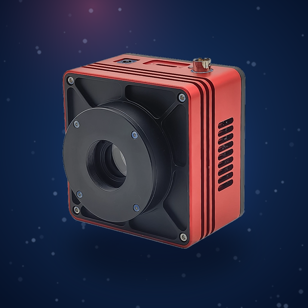
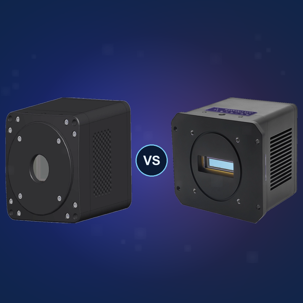
Semiconductors are widely used in communications, photovoltaic power generation, lighting, and other fields, with solar panels representing one of their most large-scale applications. Quality optimization and efficiency improvement in solar panel manufacturing processes have attracted considerable attention. Short-wave infrared (SWIR) cameras can reveal details invisible to the human eye and visible-light cameras, playing a critical role in detecting defects in solar panels and reducing production costs.
Background:
Solar panels are the core components that convert solar energy into electricity, with monocrystalline and polycrystalline silicon solar cells being the mainstream types, widely used in residential, commercial, and industrial sectors. Improving the quality and efficiency of solar panels is a key focus of solar energy research. Impurities and defects can affect the efficiency of solar cells, making rapid and accurate detection of defective cells essential for enhancing the overall efficiency of solar panels. In the manufacturing process of solar panels, the selection of silicon wafers is fundamental. Defects in silicon wafers are on the order of micrometers (μm) and nanometers (nm), which cannot be distinguished by the naked eye or visible-light cameras. SWIR series cameras play a vital role in this application.
SWIR cameras primarily image by utilizing infrared light reflected from objects. Infrared light can penetrate silicon wafers, allowing SWIR cameras to detect internal defects within the silicon.
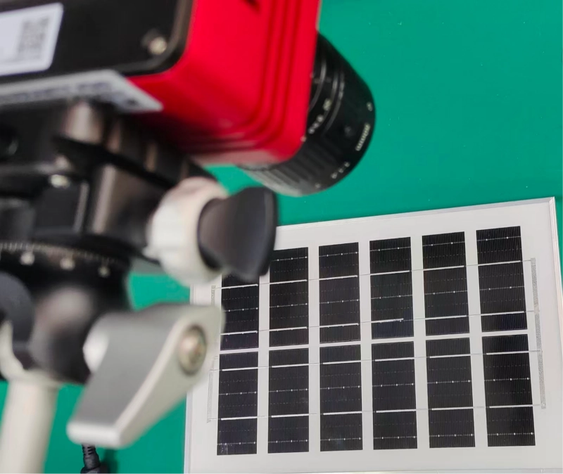
Advantages of Installing SWIR Cameras on Production Lines
Silicon Wafer/Cell Internal Defect Detection
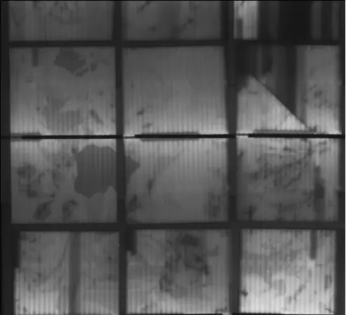
After silicon wafers absorb photon energy, they emit part of that energy in the form of electromagnetic radiation, with wavelengths around 1150 nm. SWIR cameras typically operate in the 400–1700 nm range. Therefore, using an infrared camera to image the luminescent silicon wafers can capture their glowing emissions. Microscopic physical defects on silicon wafers—such as cracks, impurities, and voids—appear as dark lines or dark areas in the image. This is the most core application of SWIR cameras. Since silicon barely absorbs infrared light above 1.1 μm, SWIR cameras can easily penetrate through the silicon wafer. For multi-layer structures, they can also identify depth information across different materials.
Solder Joint and Grid Line Inspection:
SWIR cameras can identify hot spot regions—localized overheating points that may result from incomplete soldering or material defects—which could otherwise lead to potential failures in finished products
Wafer Dicing:
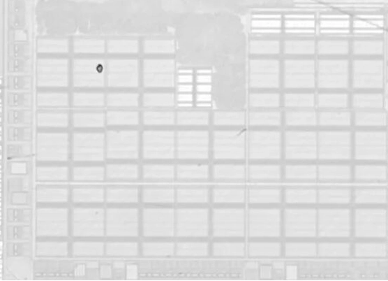
Wafer dicing can be affected by voids and impurities on the silicon wafer. Improper dicing may result in poor-quality solar panels. With the aid of infrared cameras, defects in the silicon wafers can be detected, preventing such issues, reducing costs, and improving quality.
Non-Destructive Testing:
Using infrared cameras for solar panel defect inspection requires no contact with the sample and causes no damage to the internal structure or atomic composition of the panel. It enables real-time inspection and non-destructive testing of materials.
Application Value:
SWIR cameras can characterize defects during the manufacturing process of solar cells, and rapid and accurate identification of these defects is crucial. Although such defects may not initially affect the functionality of the solar cells, their impact on reliability becomes increasingly apparent over time. Early detection of cell defects allows for timely correction, improving the quality of solar panels and reducing costs.