Blog
Latest Blog
AttosTek is a full-spectrum imaging company whose cameras, lenses, and optical systems cover everything from UV-VIS to SWIR, MWIR, and LWIR — a wavelength footprint spanning roughly 1 to 14,000 nm. This blog is where our engineers share the practical side of that technology. You will find product release announcements, experimental application reports from real research institutions, selection guides for industrial inspection and scientific imaging, and plain-English explainers on specs such as resolution, NETD, cooling, and detector materials. Whether you are evaluating a SWIR camera for silicon wafer inspection, choosing between MWIR and LWIR for a thermal imaging program, or building a custom optical system for your own application, these articles give you the data and decision framework you need before you talk to a sales engineer.
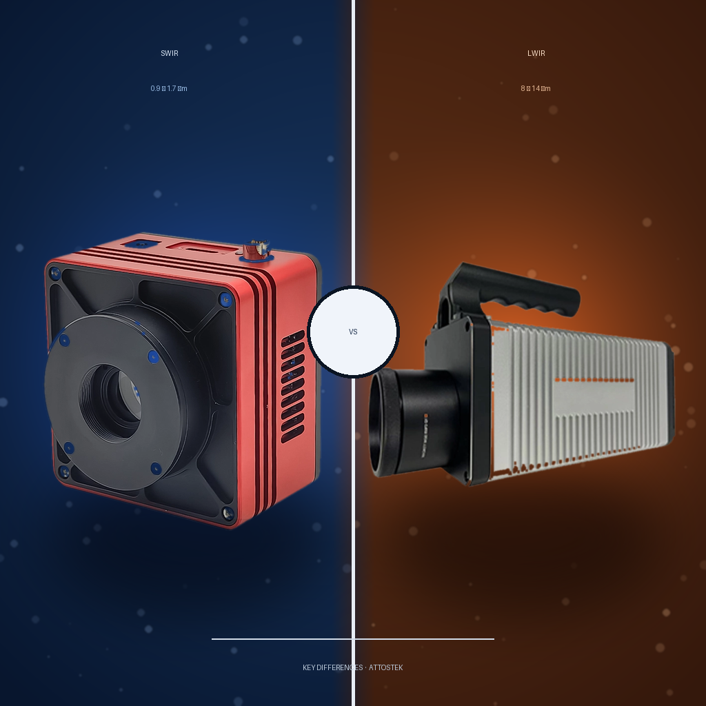
What are the key differences between SWIR and LWIR cameras?
A SWIR camera detects reflected short-wave infrared photons between roughly 0.9 and 1.7 μm and produces sharp, high-resolution images of material contrast; an LWIR camera detects thermal radiation that the object itself emits in the 8–14 μm band and produces a heat map. The difference is not one of quality but of physics: wavelength range, imaging mechanism, lens materials, cost and applications all follow from those two facts. Key Takeaways What is an LWIR Camera Module? An LWIR camera module is a complete imaging engine built around a long-wave infrared detector: the sensor, the lens interface, the drive electronics and the data interface, packaged so an OEM can drop it into a larger instrument. The band is 8–14 μm, where objects near room temperature radiate most of their energy. AttosTek's LWIR line covers the three detector families on the market — uncooled cameras based on vanadium oxide (VOx) microbolometers, cooled cameras built on mercury cadmium telluride (MCT) or type-II superlattice (T2SL), and high-operating-temperature (HOT) cooled designs — with resolutions from 640 × 512 through 1024 × 768 to 1280 × 1024 and industrial interfaces including GigE, USB 3.0, CameraLink and MIPI. The module format matters commercially. A handheld thermal imager…
10/19/2026
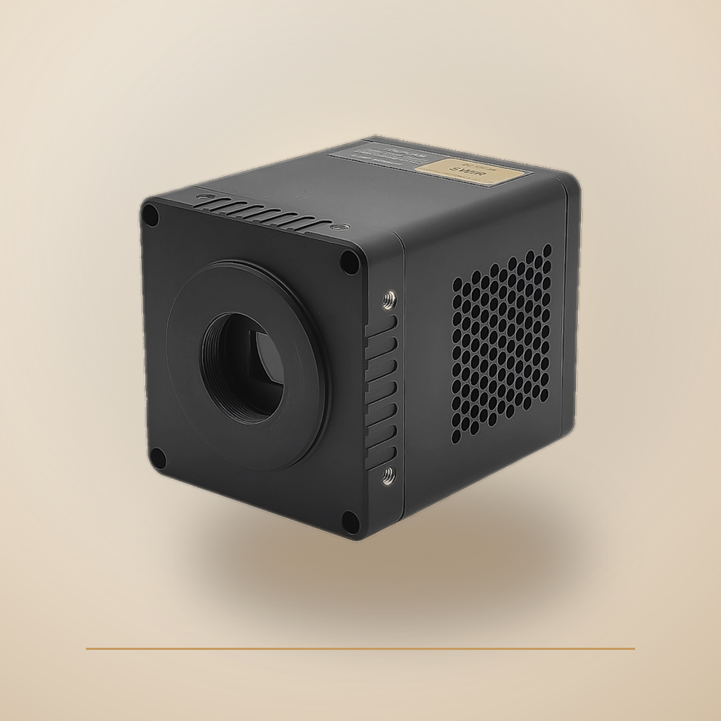
What Is a High Speed InGaAs Camera? Working Principle, Specifications, and SWIR Applications
A high speed InGaAs camera is a short-wave infrared imager that pairs an indium gallium arsenide focal plane array with a fast readout integrated circuit, letting it capture hundreds to thousands of frames per second while staying sensitive across roughly 900–1700 nm. Silicon stops seeing light near 1100 nm, yet much industrial and scientific work — laser welding, semiconductor inspection, high-throughput sorting — happens in the short-wave infrared and unfolds faster than a general-purpose SWIR camera can sample. The sensor sets wavelength and sensitivity; the readout chain and interface set speed. Key Takeaways 1. What Is a High Speed InGaAs Camera? The term describes two things at once. InGaAs is the sensor material — indium gallium arsenide, a III-V compound semiconductor whose bandgap makes it responsive to wavelengths that silicon passes straight through. "High speed" is a claim about frame rate, and it is always relative: a SWIR camera running 200 fps at full resolution is fast for this class of detector, because an InGaAs array carries far more readout overhead than a small visible-light CMOS sensor. Crop the region of interest and the same camera reaches 8000 fps. What separates a high speed InGaAs camera from a general-purpose one…
10/14/2026
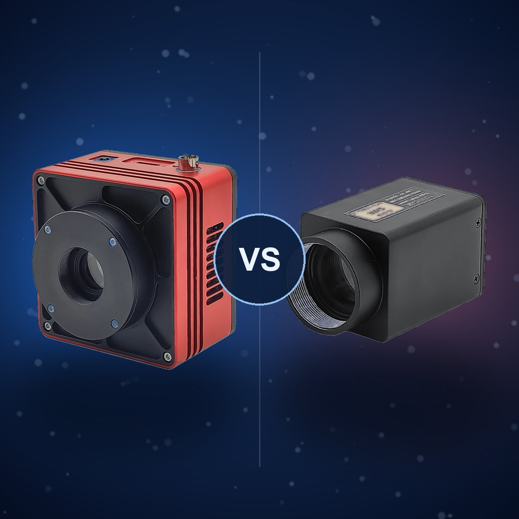
Cooled vs. Uncooled InGaAs Cameras: Impact on Noise, Exposure, and Imaging Quality
Cooling changes three things in an InGaAs camera: dark current, usable exposure time and the faintest signal you can recover. An uncooled InGaAs camera draws about 2 W, weighs tens of grams and starts instantly, which suits bright, short-exposure industrial work. A cooled InGaAs camera holds the image sensor below ambient with a thermoelectric cooler or a deep-cooled stage, cutting dark current by an order of magnitude so exposures can stretch from milliseconds to seconds. Neither design is better in the abstract — the application decides, and the numbers make the choice obvious. Key Takeaways 1. Understanding Cooled and Uncooled InGaAs Camera Technologies An InGaAs camera is built around a short-wave infrared image sensor: a two-dimensional array of indium gallium arsenide photodiodes, bonded pixel by pixel to a silicon readout integrated circuit. The photodiodes convert 900–1700 nm photons into charge, and the ROIC integrates, amplifies and digitises it. That same structure serves both designs — what separates them is how the sensor is held thermally. In an uncooled InGaAs camera the sensor sits at ambient temperature and heat leaves through the body. There is no cooler, no fan and no wait, so the camera produces an image immediately. In a…
09/28/2026
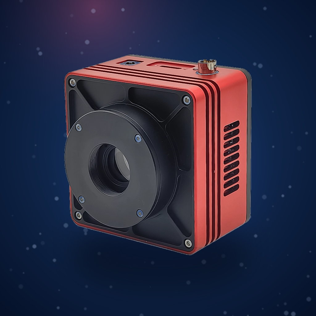
How to Choose an InGaAs SWIR Camera?
Choosing an InGaAs camera comes down to six decisions: what your application must detect, which spectral window it needs, how much resolution the target requires, what frame rate the line speed demands, whether dark current justifies cooling, and how the camera will talk to your software. InGaAs sensors cover 900–1700 nm with optional extension to 2200 or 2700 nm, and a modern InGaAs SWIR camera pairs that sensor with a silicon ROIC through indium bump bonds. This guide walks through each factor in order, with the datasheet numbers that separate one model from another. Key Takeaways What is an InGaAs Sensor? Indium gallium arsenide is a III-V compound semiconductor with the formula InxGa1-xAs. Its bandgap is set by the indium fraction, which is why a detector built from it can absorb light well beyond the reach of silicon. Standard silicon stops responding at roughly 1100 nm; InGaAs lattice-matched to an indium phosphide substrate responds from about 900 nm to 1700 nm, and raising the indium content pushes the cutoff to 2200 nm or 2700 nm at the cost of higher dark current. Inside an InGaAs camera, the sensor is not a single chip but a stack. The InGaAs layer is…
09/24/2026
How SWIR Cameras Work
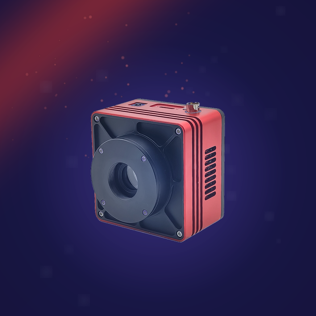
A SWIR camera images short-wave infrared — roughly 900–1700 nm — using an InGaAs focal plane array instead of silicon. Photons reflected by the target enter the lens, excite electrons in the indium gallium arsenide layer, and a readout integrated circuit (ROIC) bonded under every pixel converts that charge into a digital image. The result looks like a sharp black-and-white photograph, yet it reveals what visible and thermal cameras miss: silicon turns transparent, moisture turns dark and haze loses its grip. AttosTek builds cameras from 400 to 2700 nm with formats from 0.33 to 5 MP, in cooled and uncooled versions. Key Takeaways How do SWIR Cameras Work? A SWIR camera is a three-stage photon pipeline. Stage one is optics: the lens focuses short-wave infrared light reflected by the target onto the focal plane array, the sensor chip at the back of the camera. Stage two is detection. The FPA is a two-dimensional grid of InGaAs photodiodes, a compound semiconductor whose bandgap lets it absorb photons with wavelengths far beyond what silicon can see. Each arriving photon in the 900–1700 nm window excites an electron-hole pair, and the photodiode collects those charges as a tiny current during the exposure. Stage…
09/20/2026
CCD vs CMOS or Exmor CMOS? Which is better?
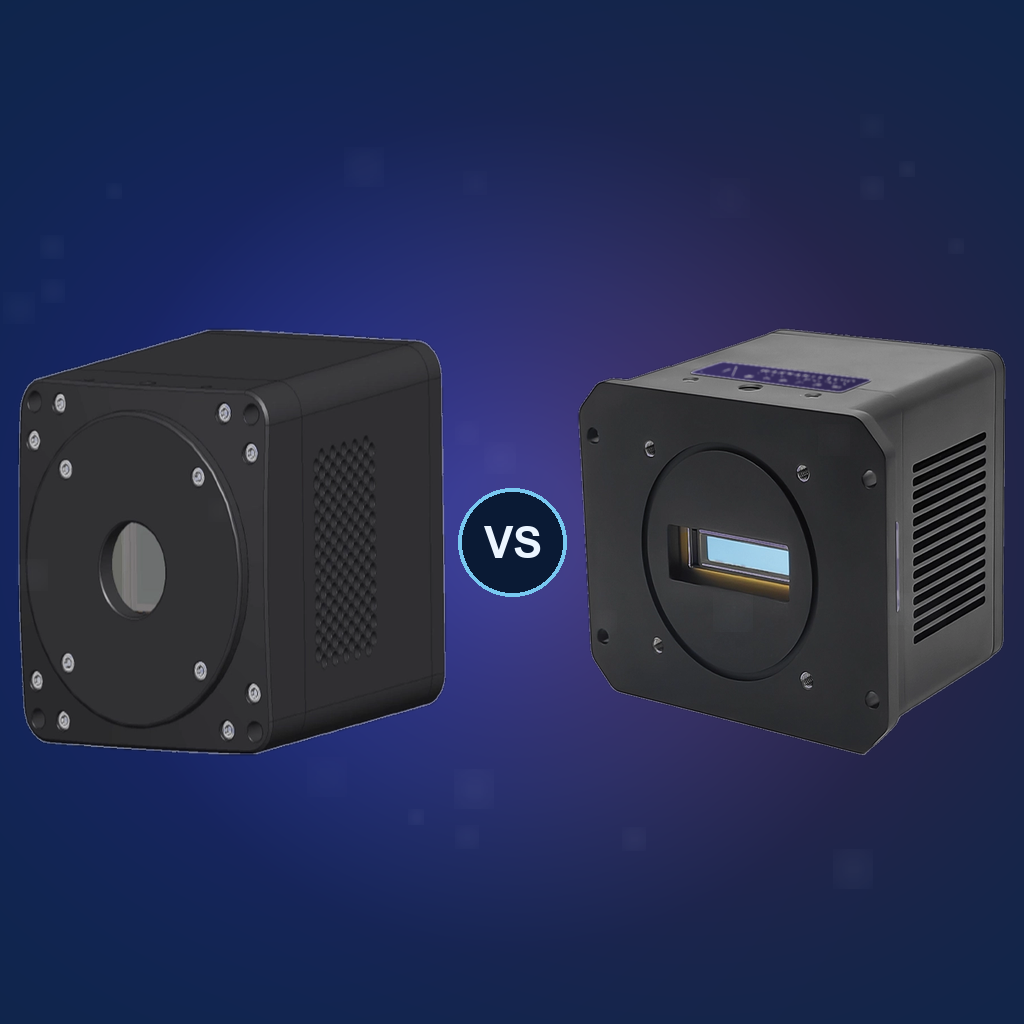
There is no single winner in the CCD versus CMOS debate, because the two sensor families optimise for different jobs. A CCD camera moves every pixel's charge to one output and reads it through a single amplifier, which rewards uniformity and low noise. A CMOS camera converts light to voltage inside every pixel and reads columns in parallel, which rewards speed, low power and integration. Modern back-illuminated scientific CMOS has closed most of the historic gap: AttosTek's flagship 4 MP 6.5 μm sCMOS camera pairs QE 95% at 450 nm with 0.72 e- read noise and 248 fps at 8-bit, so for most scientific and industrial work CMOS is now the faster and more flexible choice, while CCD sensors remain justified in a few specialised niches. Key Takeaways How CCD and CMOS Sensors Read an Image Both sensor types convert photons into charge in the same silicon, so the difference is not detection but readout. In a CCD, the charge collected by every pixel is shifted bucket-by-bucket across the sensor to a single output node, where one amplifier converts it to voltage. That single path is the CCD's superpower and its bottleneck at the same time: because every pixel passes…
09/18/2026
What is a SWIR Camera?
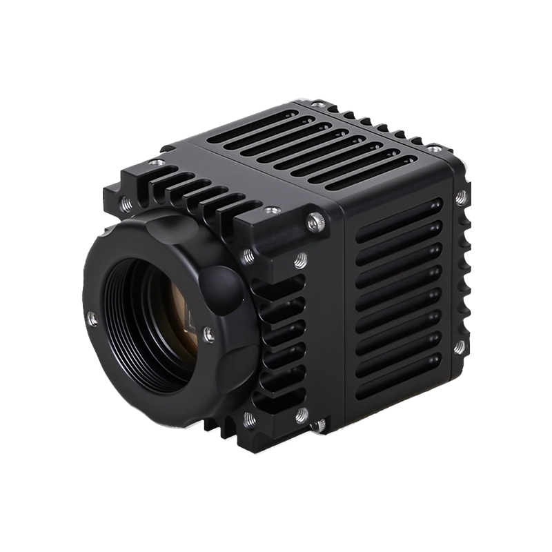
Have you ever wondered about the technology that allows us to see beyond the limits of human vision? In the modern era of advanced optics, the question "What is a SWIR Camera?" often arises among professionals and enthusiasts alike. A SWIR Camera is a specialized device designed to detect light in a spectrum that is entirely invisible to the naked human eye. Unlike standard digital cameras that rely on Visible light to produce images, this revolutionary equipment operates in a completely different Wavelength range. By doing so, a SWIR Camera can reveal hidden details and structural anomalies that traditional visual systems simply cannot detect. This remarkable ability to capture Short-wave infrared light has transformed numerous industries, proving that there is an expansive, hidden world existing right before our eyes, waiting to be discovered. Characteristics of SWIR Imaging To truly grasp the importance of this technology, we must delve into the fundamental Characteristics of SWIR Imaging. While conventional photography captures the standard Visible light we see every day, a specialized SWIR Camera functions within a distinct Wavelength range, typically spanning between 900 and 1700 nanometers. Within this unique Short-wave infrared domain, the physical properties of many common materials behave in surprising…
09/14/2026
Product Recommendation | 1.3 MP SWIR Camera SWIR051AU
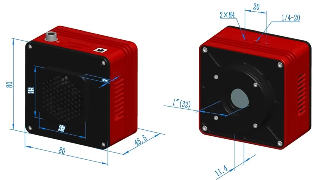
I. Product Introduction The SWIR051AU from Beijing AttosTek Co., Ltd. is a short-wave infrared (SWIR) camera with high sensitivity, high frame rate, and excellent stability. It is equipped with a Sony IMX990 sensor, featuring 1.3 MP resolution, 5 μm pixel size, and 400–1700 nm spectral response. The built-in TEC cooling system provides a 30°C temperature differential, and the USB3.0 data interface achieves a full-resolution frame rate of up to 200 fps, with a dynamic range of 58.7 dB. It is suitable for application scenarios with stringent requirements for real-time performance and detail layering, making it an ideal choice for industrial inspection, scientific measurement, and high-end vision applications such as laser imaging, spectral analysis, haze penetration, and smoke and dust environments. II. Quantum Efficiency Curve III. Filter Window Transmittance Curve IV. Camera Specifications ParameterSpecificationModelSWIR051AUSensor TypeSony IMX990 InGaAsSpectral Range400 nm – 1700 nmPixel Size5.0 μm × 5.0 μmSensor Format1/2″Frame Rate & Resolution8 Bit: 200 fps @ 1280 × 1024, 392 fps @ 640 × 51212 Bit: 108 fps @ 1280 × 1024, 209 fps @ 640 × 512Hardware Image Buffer512 MByteConversion Gain44.3 e⁻/ADUDynamic Range58.7 dBReadout Noise211 e⁻Full Well Capacity181.6 ke⁻Maximum SNR52.6 dBSensitivity121 mV / lux·sDark Current383 e⁻/s (0°C), 510 e⁻/s (10°C), 638…
09/13/2026
1700-2600nm Extended SWIR Camera Selection Recommendations
When the operating wavelength is extended beyond 1700 nm, photon energy decreases and thermal noise increases, and the SNR differences between different cameras become more pronounced. Considering imaging performance, ease of use, and price comprehensively, we recommend InGaAs cameras for imaging wavelengths not exceeding 2200 nm, MCT cameras for 2200–2600 nm band detection, and colloidal quantum dot (CQD) cameras for scenarios with sufficient illumination and lower imaging quality requirements. Comprehensive Performance Comparison of Three Camera Types Chip TypeInGaAsMCTCQDSpectral Range900–1700nm, extendable to 1900nm or even 2200nm800–2600 nm (tunable bandgap)400–2100 nm (tunable bandgap)Quantum Efficiency70%–90%70%–80%40%–60%Cooling RequirementCan operate at room temperature; extended bands require TEC cooling (–20°C to –50°C)Typically requires deep cooling (77 K to 190 K)Can be uncooled or lightly cooledDark Current~10⁴ e⁻/s/pixel<100 e⁻/s/pixel~10⁵–10⁶ e⁻/s/pixelReadout NoiseLow, <50 e⁻ModerateRelatively high, >100 e⁻CostModerate, RMB 220,000–400,000Higher, RMB 500,000–800,000Lower, RMB 100,000–300,000Process MaturityMature, mainstream technologyRelatively mature but complex processDevelopingAdvantagesSimple manufacturing process, low readout noise, high frame rate, suitable for industrial and scientific research.Excellent QE maintained at the long-wavelength end; the only stable commercial 2500 nm area array solution.Tunable spectral range, room-temperature uncooled operation, simple manufacturing process.LimitationsExtended wavelength cannot reach 2500 nm.High overall system cost, complex manufacturing process, stringent cooling requirements.Relatively high dark current, lower QE, limited in low-light…
09/13/2026
Why the Extended-Wavelength SWIR Camera SWIR1503CU-2.2 can Achieve a Spectral Response up to 2200nm?
Standard InGaAs SWIR cameras use In0.53Ga0.47As material lattice-matched to an InP substrate, with a response band of 900–1700 nm. They are now widely used in fields such as optical fiber communications and night-vision imaging. However, with the iteration of laser technology, the upgrading of high-end precision manufacturing, and the growth of application demands such as mineral exploration, extending the detection band beyond 1.7 μm has become an urgent need. The SWIR1503CU-2.2 camera launched by AttosTek is a SWIR camera extended to the 2200 nm band. Its spectrum covers 1200–2200 nm, with a QE of 70% at 1900 nm. –50°C TEC cooling effectively suppresses dark current, giving it a leading advantage among similar 2200 nm cameras. The following will analyze the technologies and processes adopted by the extended-wavelength camera. I. Adjusting the In Composition to Reduce the Bandgap The bandgap of InGaAs decreases as the In composition increases, and the absorption cutoff wavelength shifts to longer wavelengths accordingly. Therefore, increasing the In composition can extend the cutoff wavelength from 1.7 μm to above 2.2 μm. Among these, the lattice mismatch introduced by the high In composition can be suppressed through buffer layer process optimization and substrate quality control, thereby improving chip…
09/13/2026
What are the key differences between SWIR and LWIR cameras?
A SWIR camera detects reflected short-wave infrared photons between roughly 0.9 and 1.7 μm and produces sharp, high-resolution images of material contrast; an LWIR camera detects thermal radiation that the object itself emits in the 8–14 μm band and produces a heat map. The difference is not one of quality but of physics: wavelength range, imaging mechanism, lens materials, cost and applications all follow from those two facts. Key Takeaways What is an LWIR Camera Module? An LWIR camera module is a complete imaging engine built around a long-wave infrared detector: the sensor, the lens interface, the drive electronics and the data interface, packaged so an OEM can drop it into a larger instrument. The band is 8–14 μm, where objects near room temperature radiate most of their energy. AttosTek's LWIR line covers the three detector families on the market — uncooled cameras based on vanadium oxide (VOx) microbolometers, cooled cameras built on mercury cadmium telluride (MCT) or type-II superlattice (T2SL), and high-operating-temperature (HOT) cooled designs — with resolutions from 640 × 512 through 1024 × 768 to 1280 × 1024 and industrial interfaces including GigE, USB 3.0, CameraLink and MIPI. The module format matters commercially. A handheld thermal imager…
10/19/2026
What Is a High Speed InGaAs Camera? Working Principle, Specifications, and SWIR Applications
A high speed InGaAs camera is a short-wave infrared imager that pairs an indium gallium arsenide focal plane array with a fast readout integrated circuit, letting it capture hundreds to thousands of frames per second while staying sensitive across roughly 900–1700 nm. Silicon stops seeing light near 1100 nm, yet much industrial and scientific work — laser welding, semiconductor inspection, high-throughput sorting — happens in the short-wave infrared and unfolds faster than a general-purpose SWIR camera can sample. The sensor sets wavelength and sensitivity; the readout chain and interface set speed. Key Takeaways 1. What Is a High Speed InGaAs Camera? The term describes two things at once. InGaAs is the sensor material — indium gallium arsenide, a III-V compound semiconductor whose bandgap makes it responsive to wavelengths that silicon passes straight through. "High speed" is a claim about frame rate, and it is always relative: a SWIR camera running 200 fps at full resolution is fast for this class of detector, because an InGaAs array carries far more readout overhead than a small visible-light CMOS sensor. Crop the region of interest and the same camera reaches 8000 fps. What separates a high speed InGaAs camera from a general-purpose one…
10/14/2026
Cooled vs. Uncooled InGaAs Cameras: Impact on Noise, Exposure, and Imaging Quality
Cooling changes three things in an InGaAs camera: dark current, usable exposure time and the faintest signal you can recover. An uncooled InGaAs camera draws about 2 W, weighs tens of grams and starts instantly, which suits bright, short-exposure industrial work. A cooled InGaAs camera holds the image sensor below ambient with a thermoelectric cooler or a deep-cooled stage, cutting dark current by an order of magnitude so exposures can stretch from milliseconds to seconds. Neither design is better in the abstract — the application decides, and the numbers make the choice obvious. Key Takeaways 1. Understanding Cooled and Uncooled InGaAs Camera Technologies An InGaAs camera is built around a short-wave infrared image sensor: a two-dimensional array of indium gallium arsenide photodiodes, bonded pixel by pixel to a silicon readout integrated circuit. The photodiodes convert 900–1700 nm photons into charge, and the ROIC integrates, amplifies and digitises it. That same structure serves both designs — what separates them is how the sensor is held thermally. In an uncooled InGaAs camera the sensor sits at ambient temperature and heat leaves through the body. There is no cooler, no fan and no wait, so the camera produces an image immediately. In a…
09/28/2026
How to Choose an InGaAs SWIR Camera?
Choosing an InGaAs camera comes down to six decisions: what your application must detect, which spectral window it needs, how much resolution the target requires, what frame rate the line speed demands, whether dark current justifies cooling, and how the camera will talk to your software. InGaAs sensors cover 900–1700 nm with optional extension to 2200 or 2700 nm, and a modern InGaAs SWIR camera pairs that sensor with a silicon ROIC through indium bump bonds. This guide walks through each factor in order, with the datasheet numbers that separate one model from another. Key Takeaways What is an InGaAs Sensor? Indium gallium arsenide is a III-V compound semiconductor with the formula InxGa1-xAs. Its bandgap is set by the indium fraction, which is why a detector built from it can absorb light well beyond the reach of silicon. Standard silicon stops responding at roughly 1100 nm; InGaAs lattice-matched to an indium phosphide substrate responds from about 900 nm to 1700 nm, and raising the indium content pushes the cutoff to 2200 nm or 2700 nm at the cost of higher dark current. Inside an InGaAs camera, the sensor is not a single chip but a stack. The InGaAs layer is…
09/24/2026
How SWIR Cameras Work
A SWIR camera images short-wave infrared — roughly 900–1700 nm — using an InGaAs focal plane array instead of silicon. Photons reflected by the target enter the lens, excite electrons in the indium gallium arsenide layer, and a readout integrated circuit (ROIC) bonded under every pixel converts that charge into a digital image. The result looks like a sharp black-and-white photograph, yet it reveals what visible and thermal cameras miss: silicon turns transparent, moisture turns dark and haze loses its grip. AttosTek builds cameras from 400 to 2700 nm with formats from 0.33 to 5 MP, in cooled and uncooled versions. Key Takeaways How do SWIR Cameras Work? A SWIR camera is a three-stage photon pipeline. Stage one is optics: the lens focuses short-wave infrared light reflected by the target onto the focal plane array, the sensor chip at the back of the camera. Stage two is detection. The FPA is a two-dimensional grid of InGaAs photodiodes, a compound semiconductor whose bandgap lets it absorb photons with wavelengths far beyond what silicon can see. Each arriving photon in the 900–1700 nm window excites an electron-hole pair, and the photodiode collects those charges as a tiny current during the exposure. Stage…
09/20/2026
CCD vs CMOS or Exmor CMOS? Which is better?
There is no single winner in the CCD versus CMOS debate, because the two sensor families optimise for different jobs. A CCD camera moves every pixel's charge to one output and reads it through a single amplifier, which rewards uniformity and low noise. A CMOS camera converts light to voltage inside every pixel and reads columns in parallel, which rewards speed, low power and integration. Modern back-illuminated scientific CMOS has closed most of the historic gap: AttosTek's flagship 4 MP 6.5 μm sCMOS camera pairs QE 95% at 450 nm with 0.72 e- read noise and 248 fps at 8-bit, so for most scientific and industrial work CMOS is now the faster and more flexible choice, while CCD sensors remain justified in a few specialised niches. Key Takeaways How CCD and CMOS Sensors Read an Image Both sensor types convert photons into charge in the same silicon, so the difference is not detection but readout. In a CCD, the charge collected by every pixel is shifted bucket-by-bucket across the sensor to a single output node, where one amplifier converts it to voltage. That single path is the CCD's superpower and its bottleneck at the same time: because every pixel passes…
09/18/2026
What is a SWIR Camera?
Have you ever wondered about the technology that allows us to see beyond the limits of human vision? In the modern era of advanced optics, the question "What is a SWIR Camera?" often arises among professionals and enthusiasts alike. A SWIR Camera is a specialized device designed to detect light in a spectrum that is entirely invisible to the naked human eye. Unlike standard digital cameras that rely on Visible light to produce images, this revolutionary equipment operates in a completely different Wavelength range. By doing so, a SWIR Camera can reveal hidden details and structural anomalies that traditional visual systems simply cannot detect. This remarkable ability to capture Short-wave infrared light has transformed numerous industries, proving that there is an expansive, hidden world existing right before our eyes, waiting to be discovered. Characteristics of SWIR Imaging To truly grasp the importance of this technology, we must delve into the fundamental Characteristics of SWIR Imaging. While conventional photography captures the standard Visible light we see every day, a specialized SWIR Camera functions within a distinct Wavelength range, typically spanning between 900 and 1700 nanometers. Within this unique Short-wave infrared domain, the physical properties of many common materials behave in surprising…
09/14/2026
Product Recommendation | 1.3 MP SWIR Camera SWIR051AU
I. Product Introduction The SWIR051AU from Beijing AttosTek Co., Ltd. is a short-wave infrared (SWIR) camera with high sensitivity, high frame rate, and excellent stability. It is equipped with a Sony IMX990 sensor, featuring 1.3 MP resolution, 5 μm pixel size, and 400–1700 nm spectral response. The built-in TEC cooling system provides a 30°C temperature differential, and the USB3.0 data interface achieves a full-resolution frame rate of up to 200 fps, with a dynamic range of 58.7 dB. It is suitable for application scenarios with stringent requirements for real-time performance and detail layering, making it an ideal choice for industrial inspection, scientific measurement, and high-end vision applications such as laser imaging, spectral analysis, haze penetration, and smoke and dust environments. II. Quantum Efficiency Curve III. Filter Window Transmittance Curve IV. Camera Specifications ParameterSpecificationModelSWIR051AUSensor TypeSony IMX990 InGaAsSpectral Range400 nm – 1700 nmPixel Size5.0 μm × 5.0 μmSensor Format1/2″Frame Rate & Resolution8 Bit: 200 fps @ 1280 × 1024, 392 fps @ 640 × 51212 Bit: 108 fps @ 1280 × 1024, 209 fps @ 640 × 512Hardware Image Buffer512 MByteConversion Gain44.3 e⁻/ADUDynamic Range58.7 dBReadout Noise211 e⁻Full Well Capacity181.6 ke⁻Maximum SNR52.6 dBSensitivity121 mV / lux·sDark Current383 e⁻/s (0°C), 510 e⁻/s (10°C), 638…
09/13/2026
1700-2600nm Extended SWIR Camera Selection Recommendations
When the operating wavelength is extended beyond 1700 nm, photon energy decreases and thermal noise increases, and the SNR differences between different cameras become more pronounced. Considering imaging performance, ease of use, and price comprehensively, we recommend InGaAs cameras for imaging wavelengths not exceeding 2200 nm, MCT cameras for 2200–2600 nm band detection, and colloidal quantum dot (CQD) cameras for scenarios with sufficient illumination and lower imaging quality requirements. Comprehensive Performance Comparison of Three Camera Types Chip TypeInGaAsMCTCQDSpectral Range900–1700nm, extendable to 1900nm or even 2200nm800–2600 nm (tunable bandgap)400–2100 nm (tunable bandgap)Quantum Efficiency70%–90%70%–80%40%–60%Cooling RequirementCan operate at room temperature; extended bands require TEC cooling (–20°C to –50°C)Typically requires deep cooling (77 K to 190 K)Can be uncooled or lightly cooledDark Current~10⁴ e⁻/s/pixel<100 e⁻/s/pixel~10⁵–10⁶ e⁻/s/pixelReadout NoiseLow, <50 e⁻ModerateRelatively high, >100 e⁻CostModerate, RMB 220,000–400,000Higher, RMB 500,000–800,000Lower, RMB 100,000–300,000Process MaturityMature, mainstream technologyRelatively mature but complex processDevelopingAdvantagesSimple manufacturing process, low readout noise, high frame rate, suitable for industrial and scientific research.Excellent QE maintained at the long-wavelength end; the only stable commercial 2500 nm area array solution.Tunable spectral range, room-temperature uncooled operation, simple manufacturing process.LimitationsExtended wavelength cannot reach 2500 nm.High overall system cost, complex manufacturing process, stringent cooling requirements.Relatively high dark current, lower QE, limited in low-light…
09/13/2026
Why the Extended-Wavelength SWIR Camera SWIR1503CU-2.2 can Achieve a Spectral Response up to 2200nm?
Standard InGaAs SWIR cameras use In0.53Ga0.47As material lattice-matched to an InP substrate, with a response band of 900–1700 nm. They are now widely used in fields such as optical fiber communications and night-vision imaging. However, with the iteration of laser technology, the upgrading of high-end precision manufacturing, and the growth of application demands such as mineral exploration, extending the detection band beyond 1.7 μm has become an urgent need. The SWIR1503CU-2.2 camera launched by AttosTek is a SWIR camera extended to the 2200 nm band. Its spectrum covers 1200–2200 nm, with a QE of 70% at 1900 nm. –50°C TEC cooling effectively suppresses dark current, giving it a leading advantage among similar 2200 nm cameras. The following will analyze the technologies and processes adopted by the extended-wavelength camera. I. Adjusting the In Composition to Reduce the Bandgap The bandgap of InGaAs decreases as the In composition increases, and the absorption cutoff wavelength shifts to longer wavelengths accordingly. Therefore, increasing the In composition can extend the cutoff wavelength from 1.7 μm to above 2.2 μm. Among these, the lattice mismatch introduced by the high In composition can be suppressed through buffer layer process optimization and substrate quality control, thereby improving chip…
09/13/2026