Short‑wave infrared (SWIR) InGaAs detectors are widely deployed in optical communications, machine vision, spectral analysis and other fields. Nevertheless, scenarios such as laser inspection, industrial material sorting and photovoltaic quality inspection have growing demands for detection capability above 1700 nm, which cannot be satisfied by standard short‑wave infrared cameras. This article introduces three typical application scenarios for 900‑1900 nm extended‑band SWIR cameras.
I. Laser Inspection and Beam Analysis
Throughout the full lifecycle of laser‑unit R&D, production, integration and maintenance, beam‑quality measurement is critical for guaranteeing performance and reliability. Key laser parameters including spot profile and power distribution require precise measurement.
1 Laser Types, Wavelength Bands and Applications
| Typical Laser Type | Wavelength | Primary Application Fields |
|---|---|---|
| Semiconductor laser (pump source) | 808 / 915 / 976 nm | Pumping for fiber lasers and solid‑state lasers |
| Yb:YAG / Nd:YAG / Ytterbium‑doped fiber laser | 1030‑1080 nm | Material processing (cutting, welding, marking), military ranging and pointing, medical uses |
| Nd:YAG / Nd:YVO₄ laser | 1319 / 1342 nm | Medical treatment, spectral analysis, communications |
| Erbium‑doped fiber laser | 1550 nm | Optical communications, eye‑safe LiDAR, ranging |
| Thulium‑doped fiber laser | 1900 nm | Surgical medicine, atmospheric monitoring, remote sensing, material processing |
| Ho:YAG, quantum‑cascade laser (QCL) | 2000‑2500 nm | Environmental monitoring, gas detection, medical lithotripsy and soft‑tissue surgery |
2 Unique Advantages of 900‑1900 nm SWIR Cameras
Operating near 1900 nm, thulium‑doped fiber lasers leverage strong water‑vapour and carbon‑dioxide absorption features for gas sensing in atmospheric monitoring. For material processing, they deliver efficient material treatment via direct absorption by polymer materials. Accurate measurement of beam quality, power distribution and spot morphology is therefore essential. However, its core working band lies beyond the response limit of conventional SWIR cameras.
Extended‑band SWIR cameras covering up to 1900 nm enable visualised measurement of 1900 nm laser beams, delivering a vital inspection tool for thulium‑doped laser R&D, optical‑path alignment and process monitoring.
II. Industrial Material Sorting
In industrial sectors including plastic recycling, food processing, mineral exploitation and resource recovery, accurate material identification and automatic sorting are key to product quality, recycling purity and resource‑use efficiency.
1 Material Types, Characteristic Bands and Identification Principles
| Material Type | Key Characteristic Wavelength | Identification Basis |
|---|---|---|
| Cotton / cellulose | 1490 nm, 1580 nm | O‑H combination‑vibration absorption bands |
| Wool / protein fibre | 1500 nm, 1600 nm | N‑H combination‑vibration absorption bands |
| PET (polyethylene terephthalate) | 1660 nm | C‑H combination‑vibration absorption bands |
| PA (polyamide / nylon) | 1720 nm | N‑H combination‑vibration absorption bands |
| PLA (polylactic acid) | 1900 nm | Characteristic C=O (carbonyl‑group) absorption band |
| Benzene‑ring‑containing plastics (PS high‑signature region) | Near 1900 nm | Benzene‑ring C‑H combination‑vibration absorption |
| Montmorillonite (hydrous mineral) | 1900 nm | O‑H combination‑vibration absorption from crystal‑bound H₂O |
| Spodumene pegmatite (lithium ore) | 1900 nm | Absorption signatures from hydroxyl (OH) groups and water molecules |
| Natural human hair | 2000‑2200 nm | Protein N‑H‑group absorption signatures |
2 Unique Advantages of 900‑1900 nm SWIR Cameras
Biodegradable plastics such as PLA exhibit characteristic absorption near 1900 nm, a signal inaccessible to standard SWIR cameras. SWIR cameras extended to 1900 nm can distinguish biodegradable plastics from petroleum‑based plastics in real time, supporting dedicated sorting streams for biodegradable materials.
For mineral sorting, these cameras clearly capture the 1900 nm absorption signatures of hydrous minerals and spodumene pegmatite, furnishing reliable spectral evidence for ore exploration and sorting.
III. Photovoltaic Inspection
Within the photovoltaic industrial chain, defect inspection safeguards power‑generation efficiency, service lifetime and operational safety of solar panels. During manufacturing and long‑term outdoor deployment, photovoltaic cells may develop hidden cracks, chipping, dark spots, delamination, hot spots, non‑uniform diffusion and other invisible flaws. Un‑detected defects degrade output efficiency and may trigger safety hazards.
1 Inspection Categories, Characteristic Bands and Working Principles
| Inspection Type | Key Characteristic Wavelength | Inspection Principle |
|---|---|---|
| Internal‑defect inspection of silicon wafers / silicon ingots | > 1100 nm | Silicon becomes transparent above 1100 nm; SWIR light penetrates silicon to detect subsurface cracks, saw marks and other concealed defects |
| Electroluminescence (EL) inspection | Peak ~1150 nm | Energised silicon solar cells emit radiative energy peaking near 1150 nm; defective areas show reduced or altered emission for detection of hidden cracks, chipping, dark spots and more |
| Photoluminescence (PL) inspection | Peak ~1150 nm | Laser excitation induces solar‑cell fluorescence; detects hidden cracks, delamination and other defects without electrical contact |
| Material‑variation and delamination inspection | 1550‑1950 nm | Different materials display distinct SWIR reflectance‑absorption behaviour for detection of inter‑layer separation and material heterogeneity |
| Ageing / degradation analysis of encapsulant EVA | ~1730 nm | Vinyl C‑H groups in EVA produce a characteristic absorption peak at 1730 nm; peak‑intensity shifts indicate chemical degradation of EVA |
| Internal water‑ingress detection for modules | ~1900 nm | Liquid water features strong characteristic absorption near 1900 nm. SWIR illumination and reflected‑light analysis identify water intrusion inside modules |
2 Unique Advantages of 900‑1900 nm SWIR Cameras
Conventional SWIR cameras satisfy mainstream EL, PL and silicon‑wafer internal‑defect inspection workflows for photovoltaic production. Cameras extended to 1900 nm add capability for module water‑ingress testing and encapsulant‑material ageing analysis, supplying important technical support for photovoltaic‑power‑station operation and maintenance.
IV. Attostek SWIR1503CU‑1.9 Short‑Wave Infrared Camera
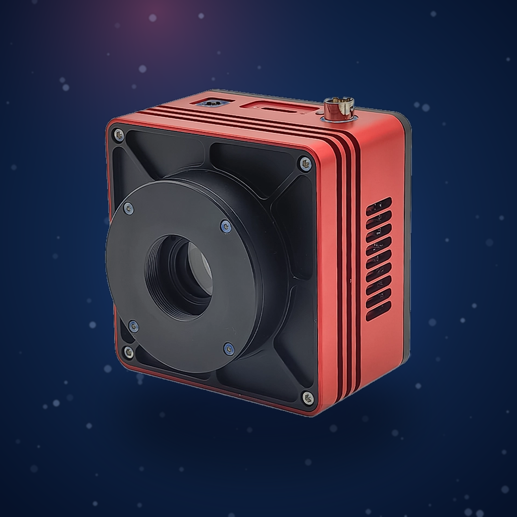
Attostek presents the SWIR1503CU‑1.9 extended‑band SWIR camera built around an extended‑response InGaAs detector. By raising the indium (In) fraction within the InGaAs absorbing layer, the material’s bandgap is narrowed, stretching spectral response from the traditional 900‑1700 nm out to 900‑1900 nm.
The unit delivers low read‑out noise, excellent pixel‑array uniformity, high‑frame‑rate imaging and broad interface compatibility. It offers a high‑performance, cost‑effective imaging solution for research‑oriented and industrial users across materials science, optical‑fiber communications, industrial quality inspection and semiconductor metrology.