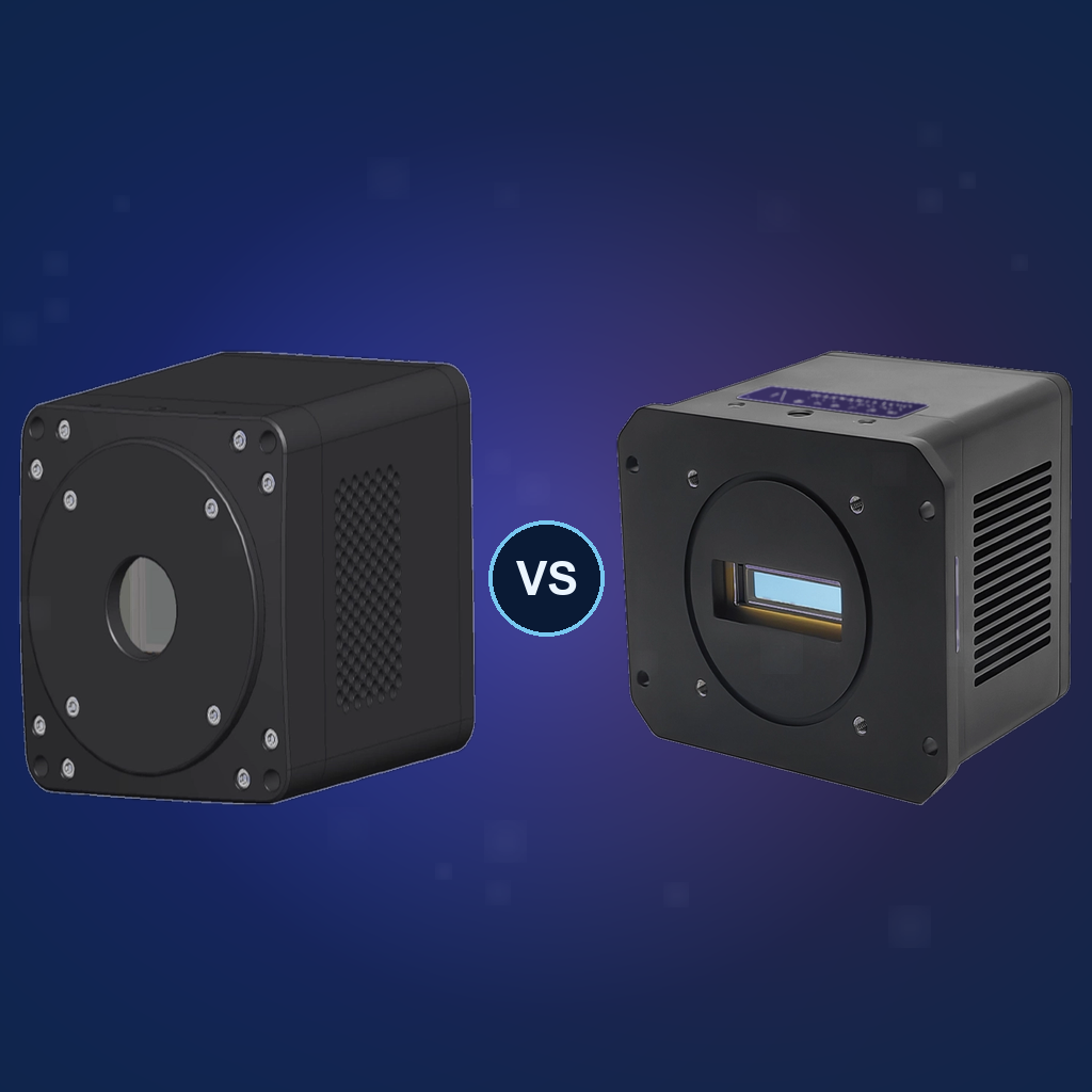
Standard InGaAs SWIR cameras use In0.53Ga0.47As material lattice-matched to an InP substrate, with a response band of 900–1700 nm. They are now widely used in fields such as optical fiber communications and night-vision imaging. However, with the iteration of laser technology, the upgrading of high-end precision manufacturing, and the growth of application demands such as mineral exploration, extending the detection band beyond 1.7 μm has become an urgent need.
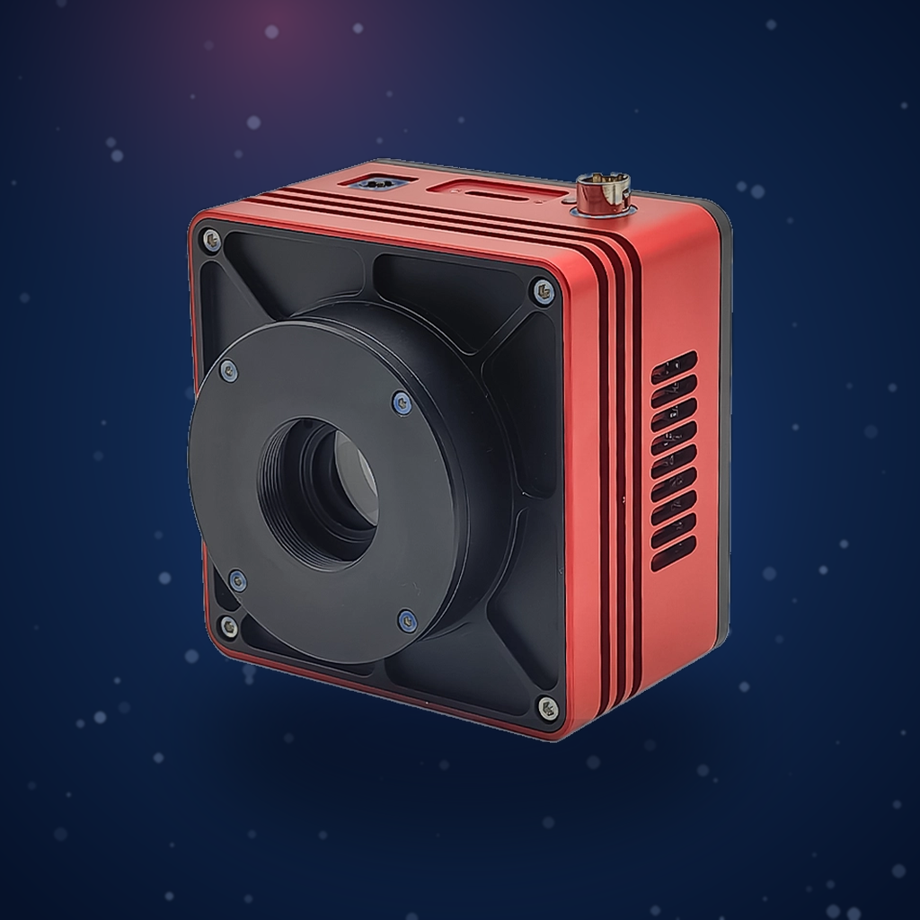
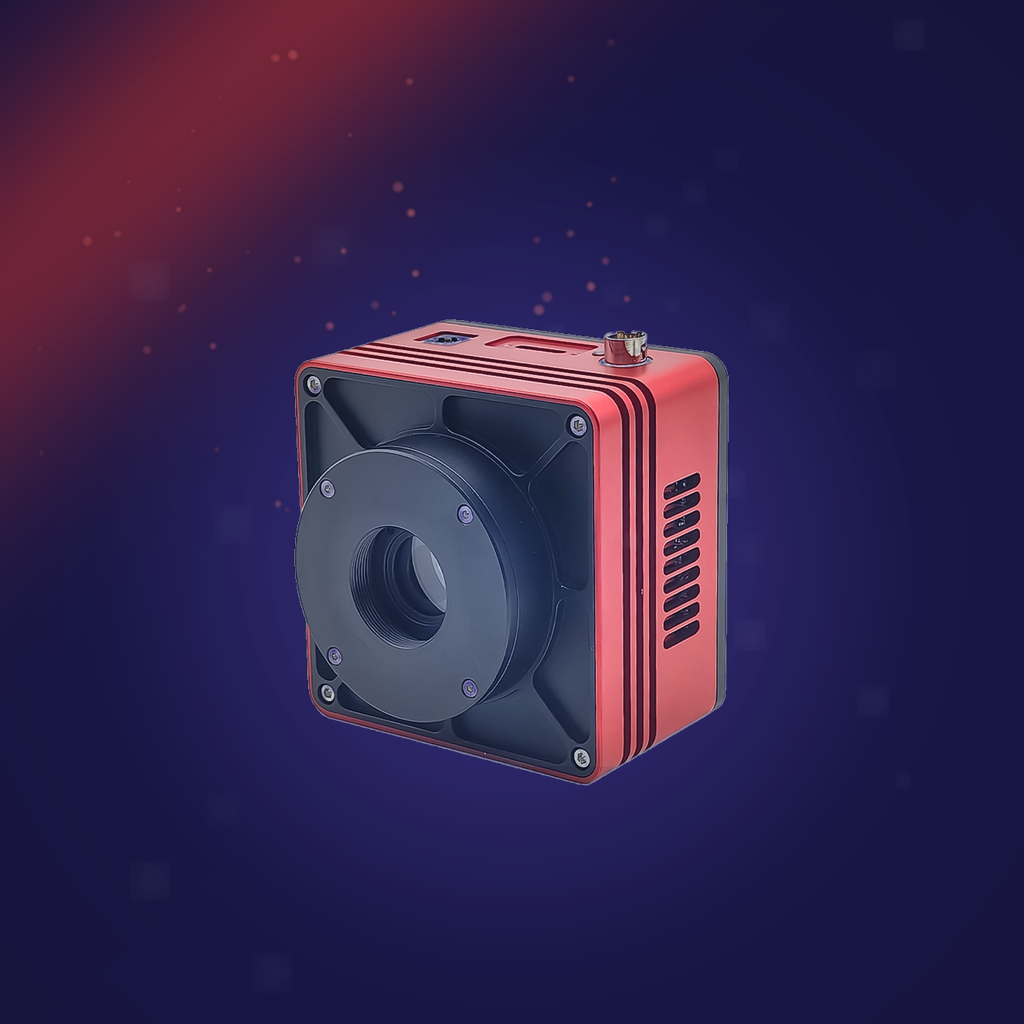
The SWIR1503CU-2.2 camera launched by AttosTek is a SWIR camera extended to the 2200 nm band. Its spectrum covers 1200–2200 nm, with a QE of 70% at 1900 nm. –50°C TEC cooling effectively suppresses dark current, giving it a leading advantage among similar 2200 nm cameras. The following will analyze the technologies and processes adopted by the extended-wavelength camera.
I. Adjusting the In Composition to Reduce the Bandgap
The bandgap of InGaAs decreases as the In composition increases, and the absorption cutoff wavelength shifts to longer wavelengths accordingly. Therefore, increasing the In composition can extend the cutoff wavelength from 1.7 μm to above 2.2 μm. Among these, the lattice mismatch introduced by the high In composition can be suppressed through buffer layer process optimization and substrate quality control, thereby improving chip performance.
II. Buffer Layer and Substrate Quality Control
1. Graded Buffer Layer Strategy
To alleviate the lattice mismatch between high-In-composition InGaAs and the InP substrate, researchers have developed various buffer layer schemes. Traditional methods include continuously graded buffer layers and step-graded continuously graded buffer layers. Studies have shown that a buffer layer structure combining step grading and continuous grading can effectively reduce material surface roughness while simultaneously suppressing device dark current. Li Wenlong et al. used MOCVD processes to grow InₓGa₁₋ₓAs transition layers with different structures on InP substrates, preparing high-indium-composition InGaAs epitaxial materials. Experimental results indicate that the transition layer structure design directly determines the surface morphology and composition uniformity of the epitaxial wafer.
2. Buffer Layer Compositional Overshoot Technology
The team led by Chen Xiaojuan at the Shanghai Institute of Technical Physics, Chinese Academy of Sciences, significantly improved the performance of a 2.2 μm cutoff wavelength In₀.₇₅Ga₀.₂₅As focal plane array by substantially increasing the overshoot composition of a linearly graded InₓAl₁₋ₓAs buffer layer. This enables the device to operate at relatively higher temperatures within the shorter <2200 nm cutoff wavelength range.
3. Substrate Roughness and Wafer Warpage Control
In addition to buffer layer design, the non-uniformity of substrate surface roughness affects the minority carrier lifetime and optical uniformity of the epitaxial layer. At the same time, stress accumulation during the growth of large-format chips can easily cause wafer warpage, impairing the precision of lithography and flip-chip bonding processes. Through strain control technology, warpage can be effectively controlled, ensuring the process yield of the 640×512 array.
III. Conclusion
The reason the SWIR1503CU-2.2 can extend its spectral response to 2200 nm fundamentally lies in increasing the In composition to reduce the bandgap and, through buffer layer and substrate quality control, effectively suppressing defects caused by lattice mismatch. This camera provides a high-performance domestic solution for industrial inspection, laser identification, and spectral analysis that require 2200 nm extended SWIR detection.
Main References:
- Chen X, Liu B, Cheng J, et al. Enhanced Performance of Extended Wavelength InₓGa₁₋ₓAs Focal Plane Arrays via Compositional Overshooting of InₓAl₁₋ₓAs Buffer Layer[J]. IEEE Journal of Quantum Electronics, 2025, 61.
- Meng Q, El-Jaroudi R H, Dadey A D, et al. Extended wavelength photodiodes in the B-III–V material system[J]. Applied Physics Letters, 2025.
- Li W, Liu L, Chen J, et al. Optimized wavelength-extended high-In component InGaAs epitaxial film with designed InAlAs transition layer structure[C]. SPIE/COS Photonics Asia, 2025.