Atomic fluorescence imaging is an effective method for characterizing atomic spatial distribution and quantum state information in fields such as ultracold atoms and quantum simulation. Depending on the wavelength of atomic fluorescence radiation, this technique can be divided into visible-light atomic fluorescence imaging and short-wave infrared (SWIR) atomic fluorescence imaging. The former is suitable for atomic systems such as rubidium, potassium, and lithium, while the latter targets metastable helium, erbium, strontium, and other atomic systems. As research expands into metastable noble gases and rare-earth atomic systems, SWIR atomic fluorescence imaging is playing an increasingly indispensable role in cutting-edge directions such as cold atom trap observation and single-atom-resolved detection. At the same time, SWIR atomic fluorescence imaging presents several technical challenges.
I. Technical Challenges of SWIR Atomic Fluorescence Imaging
1. Scarce Fluorescence Photon Count
Fluorescence power is inversely proportional to the square of the wavelength, and the atomic spontaneous emission rate also decreases with increasing wavelength. Compared with rubidium atoms in the visible band, the number of fluorescence photons emitted per unit time by atoms in the SWIR band is significantly reduced, resulting in weak effective signals reaching the camera sensor.
2. Limited Observation Time
Dynamic processes such as free expansion, lattice tunneling, and single-atom thermal diffusion occur on the millisecond timescale, with effective imaging windows typically lasting only tens to hundreds of milliseconds. It is not possible to rely on extended exposure to accumulate photons; the detector must achieve high signal-to-noise ratio imaging within the limited exposure time.
3. Noise Constraints of SWIR Cameras
The bandgap of SWIR InGaAs sensors is much narrower than that of silicon detectors, resulting in significant thermal excitation effects, with dark current increasing exponentially with chip temperature. At the same time, the detector itself has fixed readout noise, which directly raises the detection floor and limits imaging sensitivity.
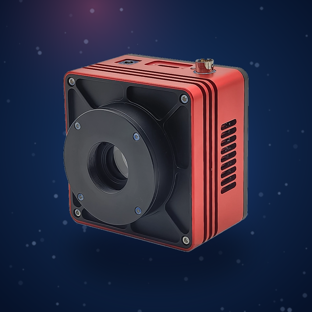
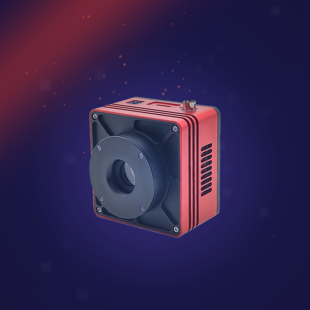
These challenges impose stringent requirements on camera quantum efficiency, frame rate, dark current, and other parameters. The Attostek SWIR1503BU SWIR camera perfectly matches the demands of SWIR atomic fluorescence imaging.
II. AttosTek SWIR1503BU Camera
1. High Quantum Efficiency
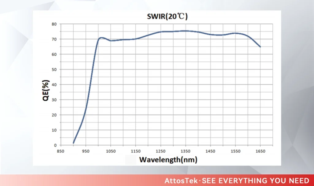
High quantum efficiency is the foundation for weak fluorescence imaging. The SWIR1503BU camera achieves a peak quantum efficiency of 75% at 1350 nm, covering a spectral range of 900–1700 nm, ensuring that incident photons are converted into photoelectrons with high probability.
2. Pixel Size and Resolution
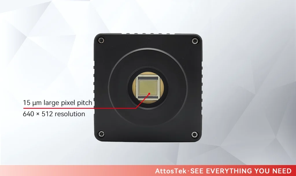
The SWIR1503BU camera features a 15 μm large pixel size, providing a larger light-sensitive area and enabling higher signal-to-noise ratio under low-light conditions. The 640 × 512 resolution fully covers conventional two-dimensional optical lattices and optical tweezer arrays, balancing micron-scale atomic spacing resolution with low-light detection sensitivity.
3. High-Speed Readout
Millisecond-scale transient processes of atoms demand high frame rates from the camera. The SWIR1503BU achieves 724 fps at 640 × 512 resolution, supporting high-speed readout in ROI mode with a readout noise of only 35.05 e⁻. Additionally, the camera supports Integrate Then Read (ITR) and Integrate While Read (IWR) modes, facilitating optimization of exposure and readout timing overlap in complex time-sequenced experiments and improving data acquisition efficiency.
4. TEC Cooling
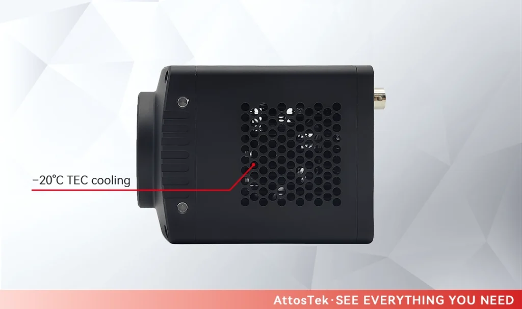
The SWIR1503BU camera employs TEC cooling to lower the sensor temperature to –20°C, thereby suppressing dark current—sufficient to meet the demands of short-exposure atomic fluorescence imaging and ensure imaging quality.
III. Summary
The Attostek SWIR1503BU SWIR camera has been successfully applied in metastable helium atom trap fluorescence imaging experiments, with its effectiveness validated in practice. Combining high photon collection efficiency, high-speed readout, low noise, and ease of system integration, this camera effectively overcomes the various technical challenges of SWIR atomic fluorescence imaging and is the preferred detection device for atomic fluorescence imaging experiments.