Short-wave infrared (SWIR) imaging technology, with its unique advantages of non-destructive testing, spectral identification, and penetrating imaging, has been widely applied in many critical fields such as precision optoelectronic inspection, geological resource exploration, and semiconductor inspection. At present, the spectral response range of mainstream SWIR cameras is generally concentrated in the 900–1700 nm standard band. However, with the iteration of laser technology, the upgrading of high-end precision manufacturing, and the improvement of mineral exploration accuracy, the characteristic spectral signals and operating bands of a large number of core detection targets have broken through 1700 nm, distributed in the 1700–2200 nm range, and standard SWIR cameras are difficult to meet the detection requirements. SWIR cameras with spectral response extended to 2200 nm have become important equipment for detecting such application scenarios.
I. Laser Spot Detection
Laser spot quality inspection is a core process in laser research and development, production, and operation and maintenance, directly determining equipment precision and operational stability. The core operating wavelength of the new generation of holmium lasers is 2000–2100 nm. With the advantages of low thermal effect and strong penetration, they are widely used in medical fields such as urological lithotripsy and soft tissue cutting. SWIR cameras extended to 2200 nm, with ultra-long wavelength response, can capture the details of holmium-doped laser spots in real time and with high precision, enabling dynamic beam quality diagnosis, and providing reliable support for the R&D debugging and mass production quality inspection of holmium-doped fiber lasers.
II. Geological Exploration
In the fields of geological remote sensing and mineral exploration, SWIR spectral technology has become a key means for rapid and accurate identification of altered minerals. Muscovite is the most widely developed altered mineral in hydrothermal deposits. The Al-OH groups of muscovite and sericite minerals have characteristic absorption peaks near 2200 nm. Relying on 2200nm extended-wavelength imaging capability, through core scanning and field remote sensing imaging, it is possible to accurately identify mineral spectral characteristics, invert mineral composition and alteration degree, and achieve efficient, high-precision refined geological exploration.
III. Semiconductor Material Layered Inspection
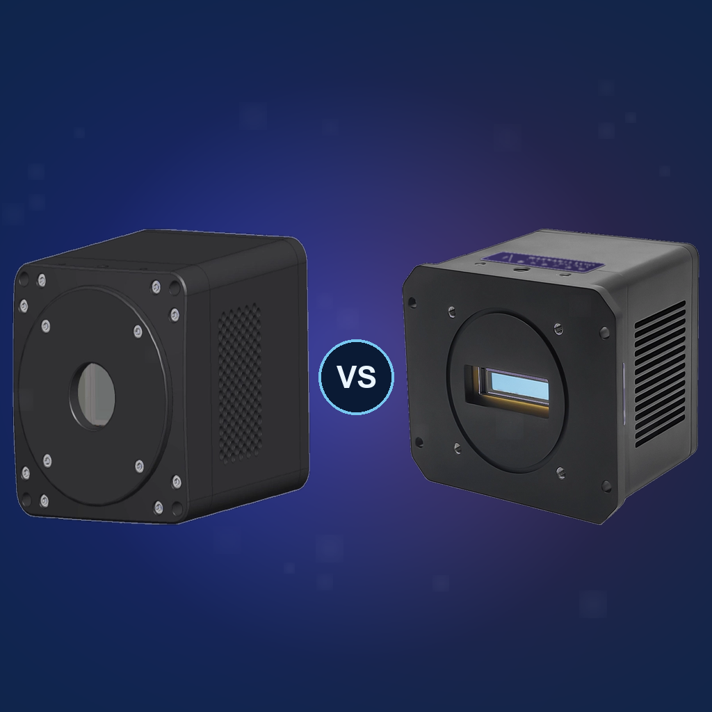
Semiconductor wafer multilayer structure inspection is a key link in chip process quality control, directly affecting chip yield. With the continuous iteration of chip stacking processes, the penetration capability of visible light and standard SWIR equipment is limited, making it difficult to identify deep hidden defects inside wafers. Compared with standard SWIR cameras, 2200nm extended-wavelength cameras can effectively cover the 1700nm–2200nm detection interval, clearly presenting the deep internal structure of wafers under non-destructive conditions, accurately identifying defects such as layer offset and uneven film thickness, and adapting to the needs of high-end wafer mass production non-destructive quality inspection and process optimization.
IV. AttosTek SWIR1503CU-2.2 Extended-Wavelength SWIR Camera
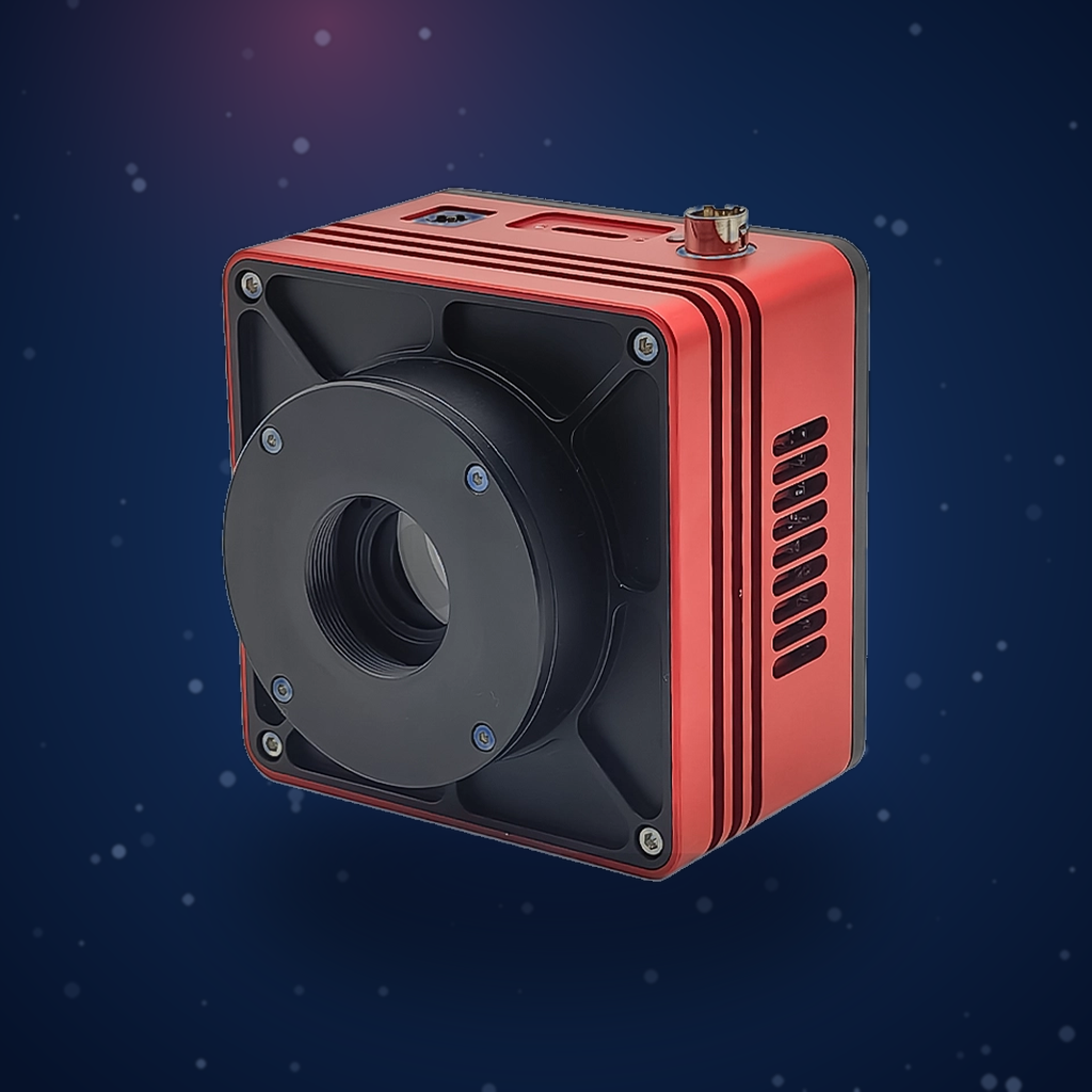
The AttosTek SWIR1503CU-2.2 extends the upper limit of spectral response to 2200nm by adjusting the indium composition ratio of the InGaAs chip, completely covering the 1200–2200nm imaging interval. It features 640×512 resolution and 15µm pixel size, ensuring the capture of fine details. At 1900nm wavelength, its quantum efficiency is as high as 70%, ensuring excellent detection sensitivity within the extended band. The device is equipped with –50°C TEC cooling, greatly suppressing dark current and improving the signal-to-noise ratio of long-wavelength weak-light imaging. The 270fps high frame rate meets the needs of real-time high-speed imaging, making it a professional imaging device with balanced performance and strong adaptability in the current 2200nm extended SWIR imaging field.