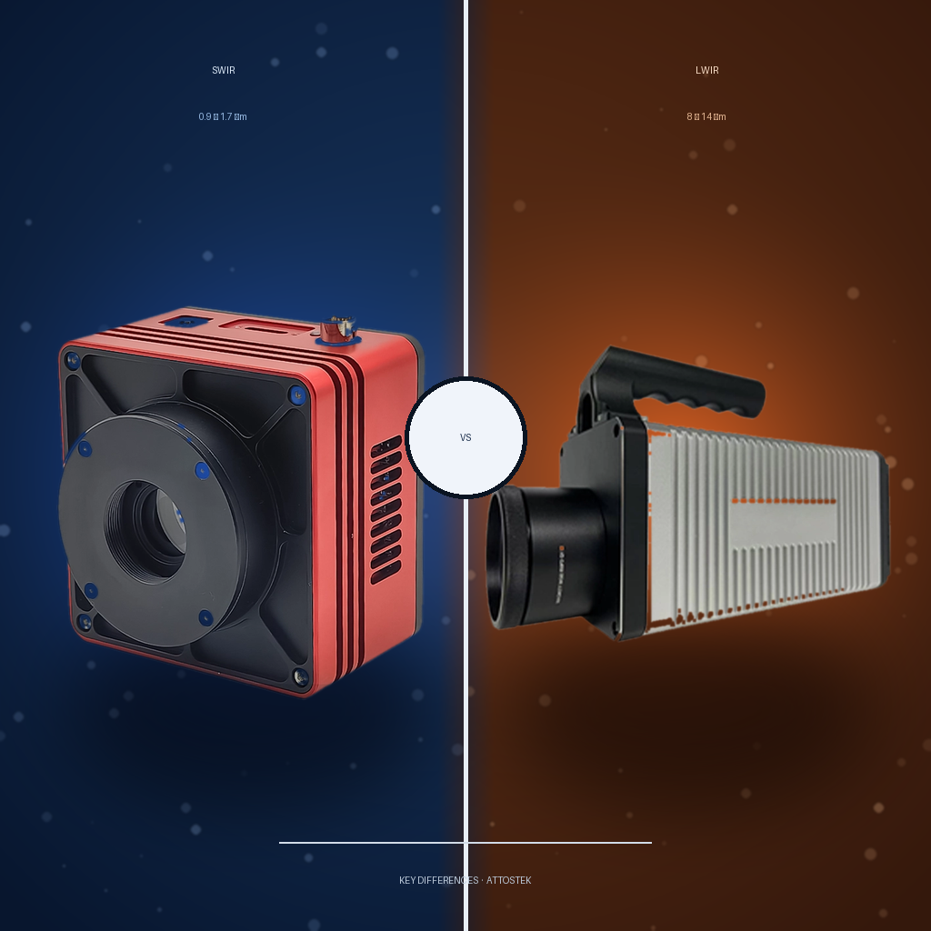
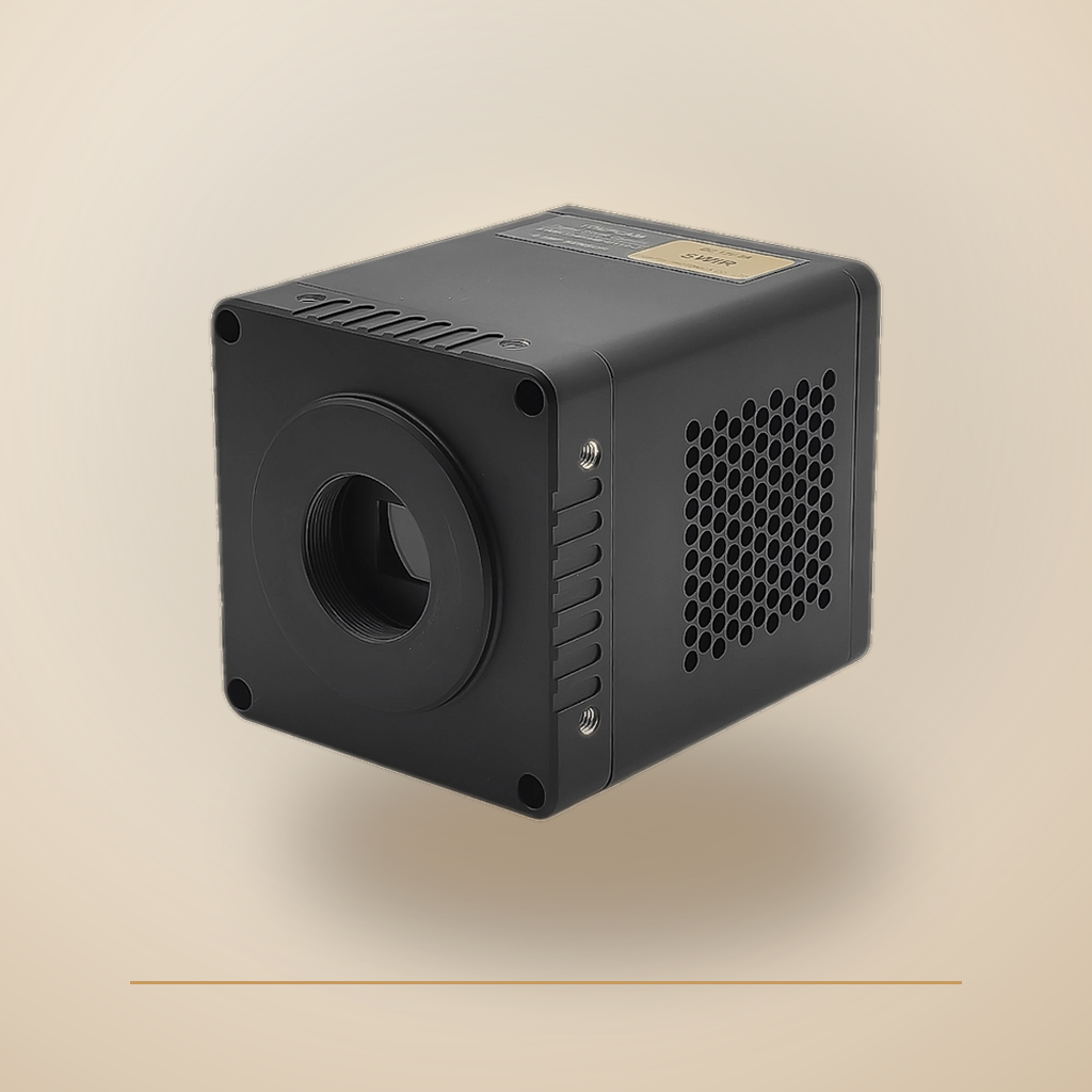
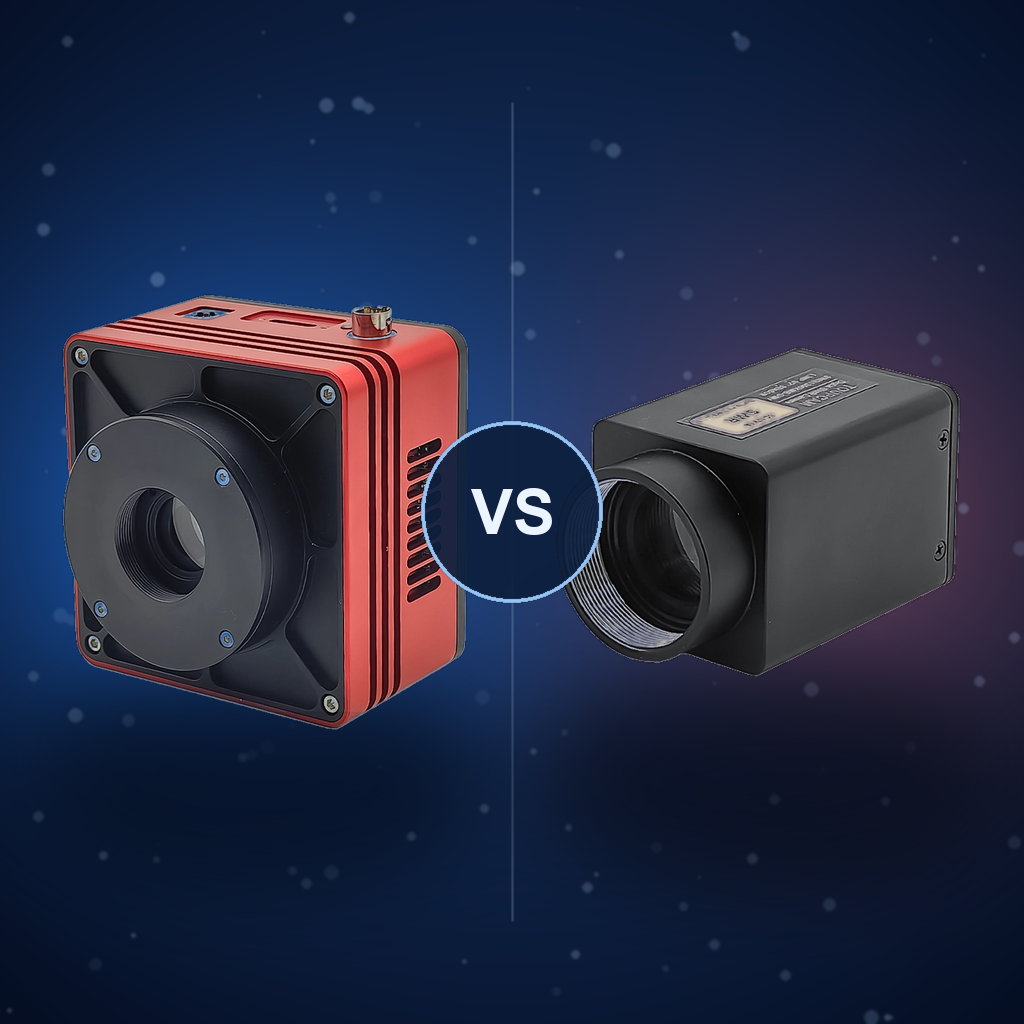
A high speed InGaAs camera is a short-wave infrared imager that pairs an indium gallium arsenide focal plane array with a fast readout integrated circuit, letting it capture hundreds to thousands of frames per second while staying sensitive across roughly 900–1700 nm. Silicon stops seeing light near 1100 nm, yet much industrial and scientific work — laser welding, semiconductor inspection, high-throughput sorting — happens in the short-wave infrared and unfolds faster than a general-purpose SWIR camera can sample. The sensor sets wavelength and sensitivity; the readout chain and interface set speed.
Key Takeaways
- The sensor sets the band, the readout chain sets the speed. An indium gallium arsenide focal plane array covers roughly 900–1700 nm, while its readout integrated circuit and data interface decide whether the camera delivers 200 or 8000 frames per second.
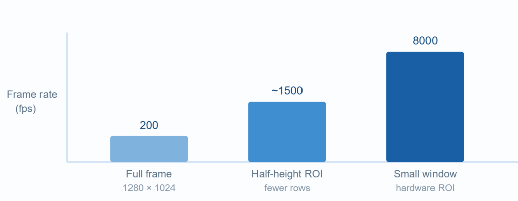
- Full-frame speed is the honest number. A 1.3 MP InGaAs camera reaches 200 fps at 1280 × 1024; the same FPA sensor climbs to 8000 fps only after the region of interest is cropped to a small window.
- Interface bandwidth caps frame rate. USB3.0 and GigE cannot carry thousands of full frames per second, so high frame rate designs lean on CoaXPress or CameraLink together with a matching frame grabber.
- Cooling protects the long-exposure end. Dark current in one 1.3 MP sensor falls from 638 e/s at 20 °C to 383 e/s at 0 °C, which keeps faint signals measurable once exposure stretches out.
- Area and linear sensors solve different problems. Area arrays capture a whole scene in a snapshot, while linear arrays scan a moving web or free-falling objects at very high line rates.
1. What Is a High Speed InGaAs Camera?
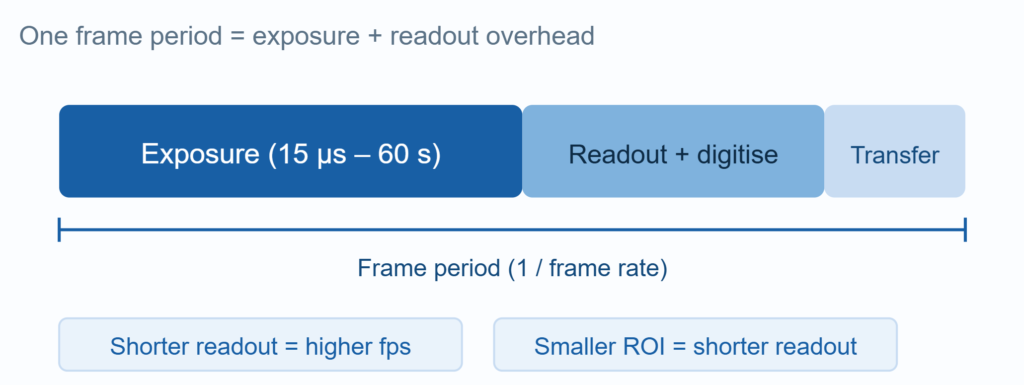
The term describes two things at once. InGaAs is the sensor material — indium gallium arsenide, a III-V compound semiconductor whose bandgap makes it responsive to wavelengths that silicon passes straight through. “High speed” is a claim about frame rate, and it is always relative: a SWIR camera running 200 fps at full resolution is fast for this class of detector, because an InGaAs array carries far more readout overhead than a small visible-light CMOS sensor. Crop the region of interest and the same camera reaches 8000 fps.
What separates a high speed InGaAs camera from a general-purpose one is not the photodiode array but everything behind it. The readout integrated circuit must integrate, amplify and digitise every pixel quickly; the on-camera electronics must push the resulting data out without dropping frames; the interface must have the bandwidth to carry it. Any weak link — a slow interface, an undersized buffer, a mismatched host computer — cancels the advantage.
2. How High Speed InGaAs Cameras Work
Inside the camera, the sensor is a hybrid stack. An indium gallium arsenide focal plane array is processed as two-dimensional photodiodes, one per pixel, and each one is connected to a matching cell in a silicon readout integrated circuit through an indium bump bond. Photons absorbed in the InGaAs generate charge; the readout integrated circuit performs integration, gain and analogue-to-digital conversion. Splitting the work lets each material do what it does best — the III-V layer handles the infrared photons, and mature silicon handles fast, low-noise readout.
Speed comes from three design choices. A global shutter exposes every pixel at the same instant and then transfers the whole frame, which removes the distortion a rolling shutter would impose on a moving object. The ROIC architecture reads the array out in parallel across many output channels, so the frame period depends on how many rows can be shifted and digitised per unit time rather than on a single serial stream. An on-chip image buffer — 512 MB in one 1.3 MP FPA sensor — absorbs bursts that exceed the interface rate. Hardware region of interest and external triggering finish the job: crop the array to the rows and columns that matter and readout time falls roughly in proportion.
3. Area vs Linear High Speed InGaAs Cameras
An area high speed InGaAs camera holds a two-dimensional focal plane array — 1280 × 1024 in a common 1.3 MP format — and exposes the whole field at once. It suits any measurement that moves in two dimensions or needs a self-consistent snapshot: impact and crash studies, droplet and spray analysis, laser spot profiling, and work where a rolling shutter would smear the geometry.
A linear InGaAs camera holds a single row of photodiodes and builds the image as the object passes, so its speed is quoted as a line rate rather than a frame rate. Linear arrays dominate web and sheet inspection — film, coated paper, textile — and free-fall sorting, where fruit or pellets cross a narrow band of illumination at production speed and a line-scan sensor catches every item without motion blur. The trade is that a linear sensor needs relative motion to form an image, so it cannot capture a stationary scene.
| Aspect | Area array | Linear array |
|---|---|---|
| Sensor geometry | 2D focal plane array (e.g. 1280 × 1024) | 1D row, one line at a time |
| Speed metric | Frames per second | Lines per second |
| How the image forms | Snapshot of the whole field | Built from motion between lines |
| Best suited to | Motion analysis, laser profiling, impact studies | Web and sheet inspection, free-fall sorting |
| Main limitation | Readout time grows with array size | Needs relative motion; no still scene |
4. Key Performance Parameters
When two high speed InGaAs cameras look comparable, the datasheet lines that decide the outcome are the ones tied to operating conditions. Maximum frame rate is meaningful only together with the resolution and region of interest it was measured at. The spectral range fixes which events are visible at all, and quantum efficiency sets how much signal you get per photon, which in turn sets the shortest exposure you can afford. Dark current governs how long you can integrate before thermal electrons swamp the image, read noise sets the floor under a single short frame, pixel pitch trades sampling density against light collection, and the interface caps the whole system. Reference values from the TEC-cooled 1.3 MP InGaAs SWIR camera in AttosTek’s A-Series, built on the Sony IMX990, are listed below.
| Parameter | What it controls | Reference value |
|---|---|---|
| Sensor | Waveband and sensitivity of the detector | Sony IMX990 indium gallium arsenide, 1/2″ |
| Spectral range | Which wavelengths reach the detector | 400–1700 nm (standard filter 400–1800 nm) |
| Resolution / pixel pitch | Sampling density vs. light per pixel | 1280 × 1024, 5.0 µm × 5.0 µm |
| Maximum frame rate | Full-frame throughput | 200 fps at full resolution |
| ROI frame rate | Speed after cropping the array | Up to 8000 fps |
| Exposure time | Freeze-motion vs. long-integration work | 15 µs – 60 s |
| Shutter | Geometric consistency on moving parts | Global shutter |
| Dark current | Usable exposure before thermal noise dominates | 638 e/s at 20 °C, 510 e/s at 10 °C, 383 e/s at 0 °C |
| Readout noise | Noise floor of a single short frame | 211 e |
| Dynamic range / SNR | Highlights and shadows in one frame | 58.7 dB / 52.6 dB |
| Interface | Bandwidth ceiling on frame rate | USB3.0 / GigE / CoaXPress / CameraLink |
| Cooling | Dark-current stability at long exposure | TEC, sensor held below ambient |
5. Why InGaAs Enables High Speed Imaging
The material is part of the reason. Indium gallium arsenide is a direct-bandgap semiconductor with a high absorption coefficient, so a thin absorbing layer converts a large share of incoming photons into charge. That high quantum efficiency means a usable signal builds up in a short exposure — and a short exposure is exactly what a high frame rate needs, so the two requirements pull in the same direction instead of fighting each other.
The detector geometry helps as well. An InGaAs photodiode can be biased so that photogenerated carriers are swept out quickly, keeping charge collection from becoming the bottleneck. Once photons are converted, the speed question moves entirely into the readout integrated circuit, and that is where silicon dominates: ROIC architecture has inherited three decades of CMOS progress, with parallel output channels, on-chip analogue-to-digital conversion, programmable gain and region-of-interest cropping. A high frame rate design is ultimately an exercise in matching a fast III-V detector to an even faster silicon readout.
6. Applications of High Speed InGaAs Cameras
Wherever a short-wave infrared event is both faint and quick, a high speed InGaAs camera earns its place. Semiconductor manufacturing is the clearest case: silicon is transparent in this band, so a focal plane array can look through a wafer or a package to find cracks, delamination and internal defects while the inspection stage keeps moving.
Laser processing is the second large family. Welding, cutting, cladding and additive manufacturing all depend on what the melt pool does in the milliseconds after the beam passes, and the short-wave infrared emission there carries temperature and geometry that a visible-light sensor cannot recover through the plume. Laser spot monitoring and beam profiling sit alongside it, where a small region of interest is usually all the frame rate you need.
Then comes high-throughput sorting, where short-wave infrared contrast separates foreign material from food on a free-fall line, identifies polymers that look identical to the eye, and catches electrode coating defects on battery lines at production speed. Research adds combustion and spray diagnostics, shock and impact tests, and microfluidic studies where the field of view is small enough for a cropped camera to run at thousands of frames per second. For visible-light work at similar rates, a 300–1000 nm high speed camera follows the same acquisition logic in the silicon band.
7. How to Choose the Right High Speed InGaAs Camera
Start from the event, not the datasheet. Estimate how long the phenomenon lasts and how far it moves while it is visible; that sets the exposure you need. If the event is a laser pulse measured in microseconds, the camera has to expose that briefly and still deliver enough signal, which points to quantum efficiency and read noise rather than to the largest frame rate on the box.
Next, decide whether you need the whole field or a strip. A full-frame 1.3 MP InGaAs camera at 200 fps is a different instrument from the same FPA sensor cropped to a small window at 8000 fps, and if your subject always sits in one part of the image, region of interest is the cheapest speed you will ever buy. Match resolution to the smallest feature you must resolve, remembering that pixel pitch and sensitivity move in opposite directions: a 5 µm pixel in a 1280 × 1024 array samples finely but collects less light per pixel than a 15 µm design, while a 5 MP 3.45 μm SWIR camera samples more finely still.
Interface and cooling close the loop. CoaXPress and CameraLink carry far more bandwidth than USB3.0 or GigE, so a camera quoted at thousands of full frames per second needs the matching frame grabber, cable and host. Cooling matters when exposure stretches past a few milliseconds, because dark current accumulates in proportion to exposure time; a TEC stage that holds the sensor below ambient keeps that term small and, just as importantly, repeatable. AttosTek supplies cooled and uncooled SWIR cameras across the A, B and C series, all with AttosView control software and an SDK covering C/C++, C#/VB.NET, Python, Java, LabVIEW, MATLAB, Micro-Manager, DirectShow and TWAIN. If a catalogue model does not fit the event, the ROIC architecture and interface can be re-specified — describe the wavelength, duration and frame rate to the AttosTek customization team for a configuration and a CIF quotation, and small-batch work is welcome.
8. Industry Trends in High Speed SWIR Imaging
Three forces are moving this category at once. The first is sensor scaling: smaller pixels in modern InGaAs focal plane arrays give more resolution per unit area, so a 5 µm pixel in a 1.3 MP format resolves finer detail without a larger optical path, and a lower cost per sensor is slowly pushing short-wave infrared onto production lines.
The second is bandwidth. As on-camera processing and faster interfaces arrive, the camera increasingly returns extracted measurements rather than raw frames — a defect flag, a centroid, a temperature trace — which shrinks the data problem that has always accompanied high frame rate work. Event-triggered acquisition, where the camera records around an external trigger, is a practical half-step for laser and impact studies where the interesting moment is brief.
The third is wavelength. Extended-response detectors push the spectral range to 2200 nm and 2700 nm for material identification where the absorption signature sits further into the infrared, while colloidal quantum dot sensors offer a lower-cost route into the same band. AttosTek builds across these directions within a portfolio spanning the full spectrum from EUV to long-wave infrared, so a multi-band program — short-wave infrared for material contrast, thermal bands for temperature — can be specified as one system rather than as unrelated purchases.
Frequently Asked Questions
What makes a camera a “high speed” InGaAs camera?
It is defined by frame rate, not by the sensor alone. Any InGaAs camera images the short-wave infrared; a high speed one adds a readout integrated circuit and interface that can move hundreds of full frames, or thousands of cropped frames, per second, which requires parallel readout channels, a global shutter and wide bandwidth.
How fast can a high speed InGaAs camera actually run?
Full-frame throughput is the honest figure for a 1.3 MP sensor: 200 fps at 1280 × 1024. Vendors also quote the region-of-interest rate, where one model in this class reaches 8000 fps in a small window. Ask which condition a headline number refers to before comparing cameras.
Do I need a cooled InGaAs camera for high frame rate work?
Not automatically. Short, bright exposures on a production line rarely need cooling. Cooling becomes necessary when exposure stretches past a few milliseconds or illumination is weak, because dark current accumulates with exposure time: one 1.3 MP sensor drops from 638 e/s at 20 °C to 383 e/s at 0 °C, which keeps long frames usable.
Which interface should I choose for high speed SWIR imaging?
Choose on bandwidth first. USB3.0 and GigE are convenient and suit moderate rates and lab use, while CoaXPress and CameraLink carry far more data and are the practical route to thousands of full frames per second. Both high-bandwidth options need a matching frame grabber and cable, so budget for those alongside the camera.
Can AttosTek customize a high speed InGaAs camera for my system?
Yes. AttosTek supports sensor, interface, cooling and housing customization even for small orders. Send the target wavelength, event duration, frame rate and resolution, and the team returns a configuration with a CIF quotation that includes freight and insurance but excludes destination duty, import tax and VAT.