A CMOS camera sensor is a semiconductor chip that converts light into a digital image. Every pixel carries its own photodiode, amplifier and readout electronics, so the chip converts and reads the array in parallel instead of shifting charge across it. That architecture is what gives a CMOS camera high frame rates, low power draw, region-of-interest readout and a choice of rolling or global shutter. At AttosTek, CMOS camera sensors cover 200–1100 nm in the visible and near-infrared, from 1.7 MP to 26 MP formats, with back-illuminated and front-illuminated options, TEC cooling and 8, 12 or 16-bit conversion.
Key Takeaways
- CMOS means complementary metal-oxide-semiconductor, and that name describes the whole design. The photodiode, amplifier, analog-to-digital converter and digital logic all sit on one semiconductor chip, so no separate readout board is needed.
- Each pixel is an active-pixel sensor. Parallel conversion is why a 4 MP CMOS camera reaches 270 fps while a 0.54 MP spectroscopy CCD delivers 12 fps, and why power stays low at high frame rates.
- Fill factor decides how much light each pixel actually collects. A 6.5 μm back-illuminated pixel puts the photodiode next to the lens, and quantum efficiency above 95% at 450 nm follows from that geometry.
- Read noise no longer settles the sensor debate. A back-illuminated sCMOS camera reaches 0.9 e⁻ read noise, so image quality now depends as much on the camera around the sensor as on the sensor itself.
- CMOS is not one wavelength band. The same architecture covers UV-VIS, SWIR InGaAs, MWIR MCT and LWIR VOx, and every band still needs its own detector material, optics and calibration.
What Is a CMOS Camera Sensor?
CMOS stands for complementary metal-oxide-semiconductor. It describes a fabrication approach that places a photodiode, a transistor amplifier, an analog-to-digital converter and digital logic on a single semiconductor chip, and it is that integration, not the light conversion itself, that defines a CMOS camera.
Light detection works the same way in every silicon sensor. A photon is absorbed in the semiconductor, the photoelectric effect frees an electron, and the electron is stored as charge in a photodiode until the readout circuit collects it. What separates sensor families is where the charge goes next, and how many pixels have to share the path.
In a CMOS sensor, each pixel site is an active-pixel sensor. The photodetector, its amplifier and its reset transistor share the same site, the amplifier converts charge to voltage on the spot, and column-level converters turn that voltage into digital numbers. Because the conversion happens in parallel across the array, the chip behaves like thousands of small cameras stitched into one die of silicon.
That parallelism also explains the low power. A charge-coupled device needs a dedicated output amplifier and usually a separate controller, while a CMOS camera can sit on a USB port and still deliver hundreds of frames per second. The camera you hold is the sensor plus a small amount of support electronics; the intelligence is in the silicon.
CMOS vs CCD Image Sensors
Both families convert photons into charge in the same silicon, so the difference is readout architecture, not sensitivity. A charge-coupled device shifts charge bucket by bucket across the array to a single output node, where one amplifier converts it to voltage. Every pixel passes through identical electronics, so pixel-to-pixel differences stay very small, and the frame has to travel in sequence.
A CMOS camera reads columns in parallel. Each pixel converts its own charge and each column has its own amplifier and analog-to-digital converter, so the array produces a digital frame with no sequential transfer step. That is the structural reason a CMOS camera reaches hundreds of frames per second, supports region-of-interest readout, and offers both rolling and global shutter.
Real numbers from AttosTek’s range make the trade concrete. The UVISI261BUG spectroscopy CCD uses an E2V CCD261 sensor with 15 μm pixels, reaching quantum efficiency of about 95% at 800 nm, and it runs at 12 fps at 2048 × 264. The 4 MP 6.5 μm back-illuminated sCMOS camera reaches quantum efficiency of 95% at 450 nm with 0.9 e⁻ read noise and 270 fps at 8-bit output.
| Parameter | CCD (charge-coupled device) | CMOS (active-pixel sensor) |
|---|---|---|
| Readout architecture | Charge shifted across the array to one output amplifier | Each pixel converts its own charge; columns read in parallel |
| Frame rate, same supplier’s reference units | 12 fps at 2048 × 264 | 270 fps at 2048 × 2048 |
| Quantum efficiency | About 95% at 800 nm | 95% at 450 nm |
| Read noise | Low, single shared amplifier | 0.9 e⁻ on a back-illuminated sCMOS design |
| Shutter | Global | Rolling or global, model dependent |
| Region-of-interest readout | Not available | Available, with binning on most models |
| Where it still wins | Precision photometry, deep-depletion designs that keep response beyond 900 nm | Frame rate, large formats, low power, system integration |
Two CCD advantages survive: the uniformity of a single charge-transfer path, which suits precision photometry, and deep-depletion silicon, which keeps useful near-infrared response alive past 900 nm where standard silicon dies. Outside those niches, the charge-coupled device has become the harder option to justify, because the camera around the sensor now decides more than the sensor does. A CMOS camera is now chosen on frame rate and image quality together, not on the label of the architecture. Where the two architectures sit side by side, our comparison of CCD and Exmor CMOS works through the readout, sensitivity and cost differences that decide the choice.
The Geometry of a CMOS Image Sensor
The geometry of a CMOS image sensor is a set of trade-offs inside a square of silicon. An active-pixel sensor places a photodetector, several transistors, a reset device and the metal interconnect that carries the signal out inside a single square of silicon. Every element needs area, and the area left for the photodetector sets the fill factor, the share of each pixel that actually collects light.
In a front-illuminated sensor the interconnect layer sits between the incoming light and the photodiode, so part of the photon stream is reflected or absorbed before it can be converted. The photoelectric effect itself behaves identically in both arrangements; only the path of the light changes. Turning the substrate around so light enters from the back removes that obstacle. That is the entire idea behind a back-illuminated sensor, and it is why a 6.5 μm back-illuminated pixel can hold quantum efficiency above 95% in the visible band without changing the pixel size.
Pixel size follows from the same geometry. A larger pixel carries more full-well capacity and collects more photons per frame, which helps when the light budget is thin. A smaller pixel puts more resolution into a given sensor area. The trade is fill factor and well capacity against sampling density, and the fill factor falls as the in-pixel electronics grow.
| Model | Sensor and geometry | Spectral range | Readout and cooling |
|---|---|---|---|
| 4 MP sCMOS (UVISI064BU10G) | 2048 × 2048, 6.5 μm, back-illuminated GSENSE6504BSI | 200–1100 nm | USB 3.2 and 10GigE, -20 °C air or -35 °C water cooling |
| 1.7–26 MP CMOS | 3.76 μm / 4.5 μm / 9 μm, Sony Exmor, rolling or global shutter | 200–1100 nm | USB 3.0 at 5 Gbit/s, two-stage TEC to -22 °C |
| 16 MP sCMOS (VIS0916FUCL) | 4096 × 4096, 9 μm, 3.2-inch GSENSE4040 | 300–1000 nm, peak QE 73.94% at 600 nm | USB 3.0 and CameraLink dual output, 1024 MB cache |
| 8.3–21 MP microscope CMOS | 3.3 μm / 2.4 μm / 2.9 μm, Sony IMX472 / IMX383 / IMX585 | 400–1000 nm with IR-CUT or dual AR coating | USB 3.2 Gen 2 at 10 Gb/s, up to 240 fps, C-mount |
Design Considerations for a CMOS Image Sensor
Five groups of numbers decide whether a CMOS camera will hold up in your process, and the spec sheet is where you should look for them. Start with image quality: read noise, quantum efficiency, full-well capacity and dynamic range. A 4 MP sCMOS camera at 0.9 e⁻ read noise and 95% quantum efficiency at 450 nm has very little left for the camera electronics to spoil, while a large-pixel format trades frame rate for photons per frame. The limits of that trade are set by the way quantum efficiency in scientific cameras is measured and by the fill factor described above. The next group is the analog-to-digital converter. 8-bit output is fast and compact, 12-bit is the working default for most scientific work, and 16-bit is for the weakest signals; the real dynamic range is the bit depth multiplied by the conversion gain in electrons per ADU, and the AttosTek 16 MP sCMOS goes further with a 12-bit and 16-bit combined HDR mode.
Shutter mode decides whether moving parts stay in place. A global shutter exposes all pixels at once, a rolling shutter exposes row by row, and on a 16 MP sCMOS the two options sit on the same body. Next comes cooling. Uncooled sensors are simpler and cheaper, TEC cooling holds the detector at a set offset below ambient and stabilises dark current for long exposures; the 1.7–26 MP CMOS family holds -22 °C at an ambient of 20 °C with a two-stage TEC, and the 4 MP sCMOS reaches -35 °C with water cooling. Finally, look at readout and signal processing: region-of-interest readout, binning, a 512 MB or 1024 MB frame buffer and the on-chip digital logic that handles the signal processing, correcting column noise and fixed-pattern noise before the data leaves the chip. That correction is what protects image quality on models with many parallel columns.
Interface choice closes the loop. USB 3.0 at 5 Gbit/s covers a 4 MP camera comfortably, USB 3.2 Gen 2 at 10 Gb/s covers high-bandwidth microscope work, 10GigE and CameraLink carry the largest frames. Every one of these cameras ships with AttosView and an SDK for C/C++, C#/VB.NET, Python, Java, LabVIEW, MATLAB, Micro-Manager, DirectShow and TWAIN, so the sensor is rarely the part that blocks integration. When frame rate and exposure time have to be balanced against each other, the relationship between frame rate and exposure time sets out the arithmetic that follows.
The Future of CMOS Image Sensors
A complementary metal-oxide-semiconductor sensor is still improving along three lines that matter for industrial and laboratory work. The first is moving more electronics into the pixel. On-chip signal processing near the source reduces the noise that once dominated the column amplifiers, and it lets the camera apply correction while the frame is still in the sensor rather than after transfer.
The second line is better light access. Back illumination is now standard in scientific sensors, and the remaining gains come from thinner interconnect layers and refined microlens arrays that steer more of the incoming photons into the photodiode, which is the same lever that defines fill factor.
The third line is time resolution. Structures that measure arrival time, photon-counting operation and stacked integration, where the logic layer sits behind the pixel layer instead of beside it, all widen the gap between what a sensor can do and what a laboratory wants to do with it. Stacking matters because it removes in-pixel electronics from the light path entirely, so fill factor stops being limited by the readout circuit.
The practical conclusion is that a CMOS image sensor is no longer a compromise for scientific work. Back-illuminated designs now match charge-coupled device uniformity in the visible band, and they add frame rate, low power and system features that no charge-coupled device can offer. What determines the result is the band, the cooling, the interface and the software around the sensor.
Where CMOS Camera Sensors Fit at AttosTek
At AttosTek the CMOS camera sensor is one member of a full spectral family, not a standalone product line. In the UV-VIS band the CMOS range runs from a 4 MP 6.5 μm back-illuminated sCMOS camera to a 1.7–26 MP CMOS camera with selectable pixel sizes, plus a 16 MP sCMOS camera for multispectral work and an 8.3–21 MP USB 3.2 CMOS microscope camera built for high-speed microscopy. Each one is the same silicon architecture viewed through a different window. Every one of them is a CMOS image sensor built on the same active-pixel structure, where a semiconductor chip carries a photodetector, an amplifier and the digital logic on one die. For a shortlist by model, our guide to five mainstream high-sensitivity and high-speed sCMOS cameras sets out where each of these formats sits against the others.
The same architecture reappears further out in the spectrum, with different detector materials: InGaAs for the short-wave infrared, MCT for the mid-wave, and VOx for long-wave. How SWIR cameras work sets out the short-wave case in detail, where the silicon photodiode is replaced by an indium gallium arsenide one and the useful range shifts to 900–1700 nm. That continuity is useful for multi-band inspection programs, because one software stack and one SDK can drive the whole set. If your requirement needs a band the standard catalogue does not cover, the AttosTek customization team works on sensor, interface, cooling and housing changes for small quantities, and the AttosTek lens and optical system lines supply the optics that match the chosen band.
CMOS Camera Sensors from AttosTek
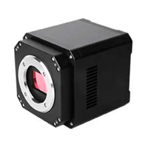 4 MP 6.5 μm back-illuminated sCMOS camera 2048 × 2048, 200–1100 nm
QE 95% at 450 nm, 0.9 e⁻ read noise USB 3.2 and 10GigE, -35 °C water cooling |
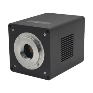 1.7–26 MP CMOS camera 3.76 / 4.5 / 9 μm pixel options, 200–1100 nm
Rolling or global shutter, 8 / 12 / 16-bit USB 3.0 at 5 Gbit/s, TEC to -22 °C |
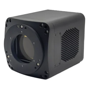 16 MP sCMOS high-resolution camera 4096 × 4096, 9 μm, 300–1000 nm
Peak QE 73.94% at 600 nm, 1024 MB cache USB 3.0 and CameraLink dual output |
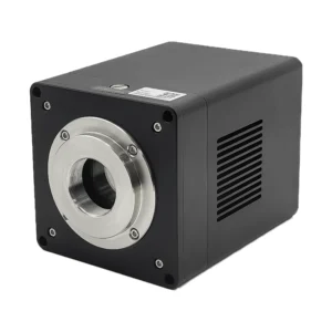 8.3–21 MP USB 3.2 CMOS microscope camera 2.4 / 2.9 / 3.3 μm, Sony IMX sensors, 400–1000 nm
USB 3.2 Gen 2 at 10 Gb/s, up to 240 fps C-mount, hardware and software binning |
Why Work with AttosTek
| Complete product range | Quality excellence | Flexible customization | Timely service |
|---|---|---|---|
| Cameras, lenses and optical systems from EUV to LWIR, 1–14,000 nm, so a multi-band program stays with one supplier. | Every unit is tested before it ships, with CE and FCC certification on the range. | Sensor, interface, cooling and housing changes are supported, including small quantities. | Technical support runs 7 × 24, with replacement and return handled by the same team. |
Frequently Asked Questions
Is a CMOS camera always the better choice over a CCD camera?
No. A CMOS camera wins on frame rate, power, format size and system features, and modern back-illuminated designs match a charge-coupled device on quantum efficiency and uniformity. A CCD still makes sense for precision photometry that depends on a single charge-transfer path, and for deep-depletion silicon that keeps near-infrared response alive beyond 900 nm.
What pixel size and resolution should I specify for a CMOS camera?
Work from the light budget. Larger pixels collect more photons and give higher signal-to-noise in dim conditions, while smaller pixels deliver more sampling points for a given field of view. Then match the lens: a 6.5 μm pixel pairs with standard C-mount optics, 3.76 μm formats need short working distances.
Does a CMOS camera need cooling, and what does TEC cooling buy me?
Cooling is optional but usually worthwhile. A thermoelectric cooler holds the sensor at a fixed offset below ambient, which lowers dark current and keeps the response stable across long exposures. AttosTek CMOS cameras run uncooled where the duty cycle allows it, and reach -22 °C with two-stage TEC or -35 °C with water cooling when the measurement needs it.
Can you supply a CMOS camera with a custom interface, trigger or housing?
Yes, and this is routine rather than exceptional. The customization process starts with the application and the optical constraint, moves to sensor, interface, cooling and mechanical changes, then to software and validation, and ends with production and delivery. USB 3.0, USB 3.2, 10GigE, CameraLink, CoaXPress and GigE interfaces, external trigger control, binning and specific form factors are all available, and small quantities are supported.
What should I send AttosTek to get a quotation for a CMOS camera?
Six items are enough for a firm quote: the application, the wavelength range, the resolution and frame rate, the interface, the cooling requirement and the environment. Add a sample or reference image if one exists, since it usually shortens the selection. Quotes are CIF and exclude destination customs duties and VAT, with 50 USD shipping inside Asia and 100 USD elsewhere.


