Experiment Title: Calcium ion fluorescence imaging
Institution: Innovation Academy for Precision Measurement Science and Technology
Experiment Date: March 2026
Ⅰ. Application Background
Ion optical clock is currently the most precise timekeeping device in the world. It traps a single ion in a vacuum and uses lasers to detect the optical signals generated during transition between specific energy levels, using the fixed frequency electromagnetic waves emitted or absorbed during these energy level transitions as a reference. The calcium ion optical clock with the highest reported uncertainty index can reach 4.4×10⁻¹⁹, which corresponds to an error of no more than one second over approximately 72 billion years. This extreme precision allow it to be applied in modern technologies such as global positioning systems and synchronized communication networks.
The working wavelength of the calcium ion optical clock is in the visible light range. Calcium ion fluorescence imaging can easily determine the number of calcium ions trapped in the optical clock. It also can monitor whether there is any position exchange of dark ion through the fluorescence imaging positions of the calcium ions.
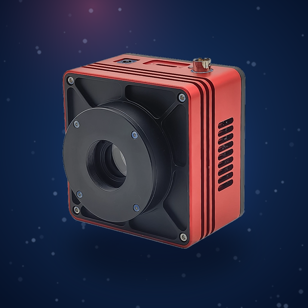
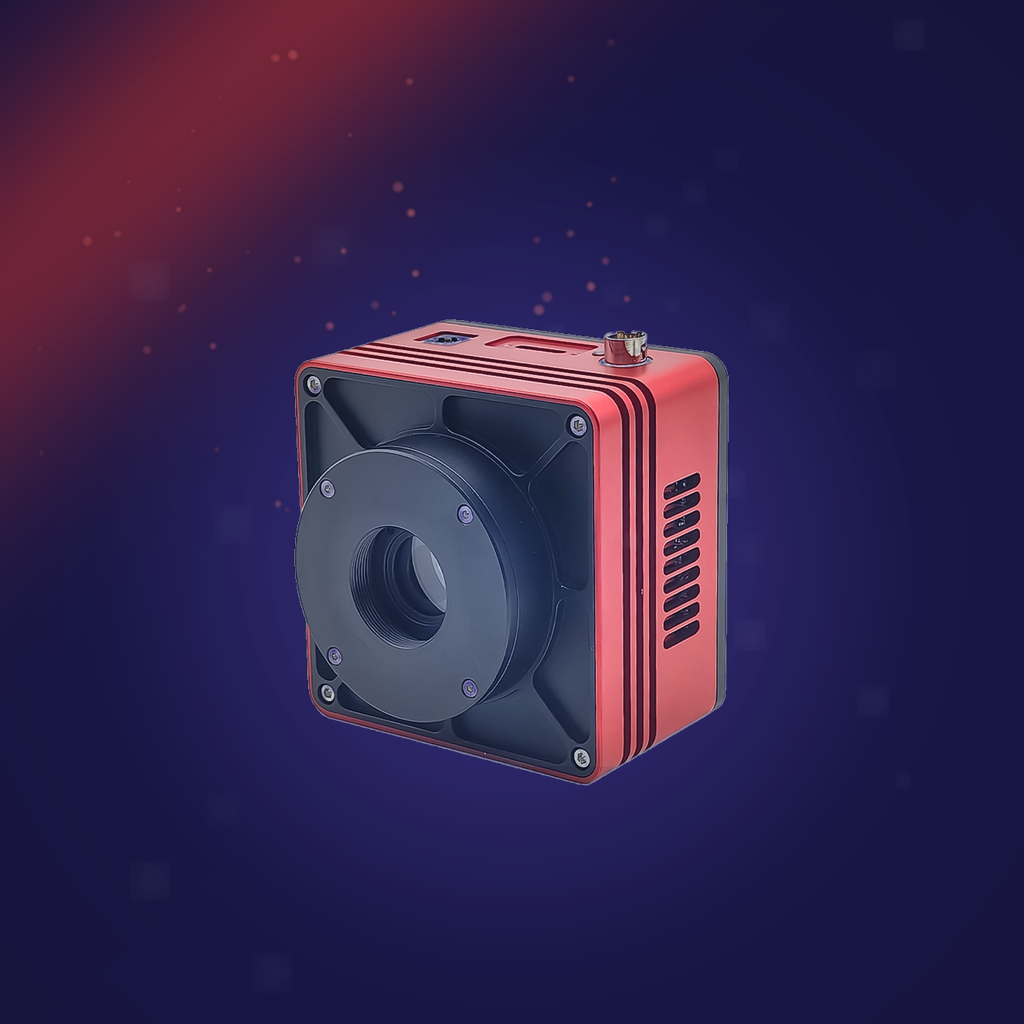
Therefore, the camera is required to have high SNR, high quantum efficiency, high sensitivity and other performance characteristics. The Attostek UVISI1605BU camera has a pixel size of 16 μm, with a maximum SNR of 49.51 dB at low conversion gain, reaching maximum quantum efficiency of 95% at a wavelength of 560 nm. The sensitivity can reach 6.4×10^8 (e-/((W/m2)·s)).
Ⅱ. Task Description
Capture images of calcium ion fluorescence imaging using a high sensitivity camera.
The calcium ion optical clock requires manipulation of trapped single ions using lasers. In this process, whether energy level transition occur in the ion is determined by the fluorescence signal from spontaneous emission of calcium ions. Therefore, a fluorescence imaging system is needed to collect the spontaneous fluorescence of calcium ions and to assess the state and number of trapped calcium ions through fluorescence imaging.
Ⅲ. Testing Equipment and Main Parameters
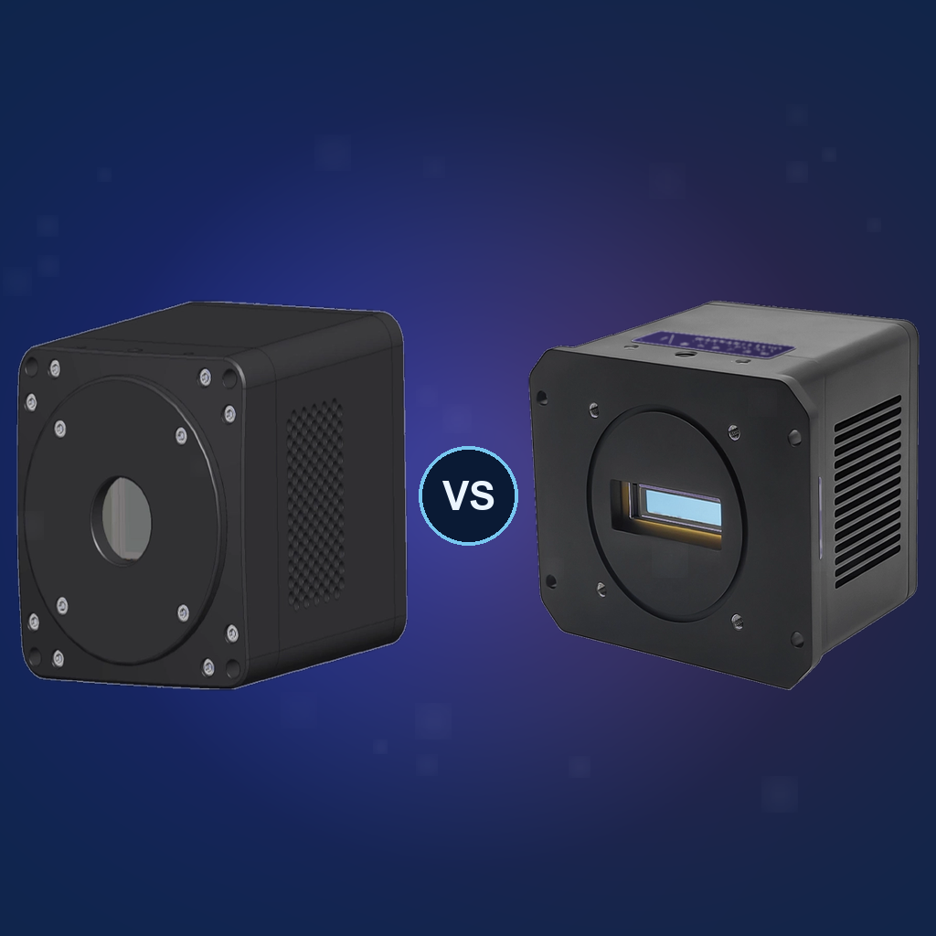
1、Camera:Attostek UVISI1605BU Camera
2、Light source:Toptica Semiconductor laser
Ⅳ.Experimental Process
1. Generate an ion trapping field.
2. Cool calcium ions with laser passing through the center of the ion trap.
3. Produce calcium ions by sputtering laser.
4. Determine whether calcium ions are produced through imaging.
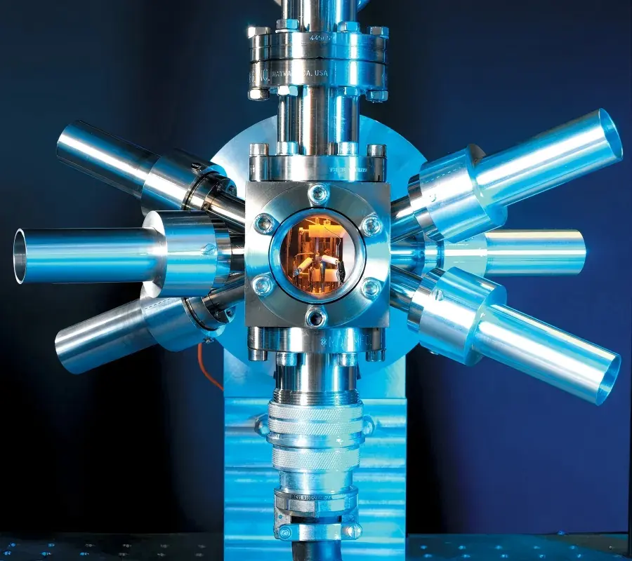
Low-temperature single-ion optical atomic clock

Ⅴ. Experimental Results and Analysis
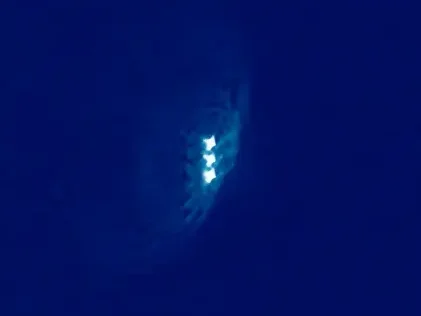
The experiment successfully obtained clear bright spots, with distinct contrasts between light and dark in the image. The positions of the bright spots indicate the locations of ions in the ion trap. Imaging can determine whether the calcium ions have crystallized, and the number of bright spots can be used to identify the number of calcium ions. This demonstrates that the UVISI1605BU camera has stable performance, high SNR, and high sensitivity, effectively meeting the application requirements of this scenario.