4MP, 6.5µm Pixel, 200-1100nm sCMOS Camera
| Features |
| The spectral response range covers 200–1100 nm. |
| 2048×2048 resolution,6.5μm pixel size |
| Roller Shutter / Global Reset |
| 11-bit ADC / 12-bit ADC / 16-bit combined HDR |
| Supports external I/O trigger control |
| 4Gb (512MB) RAM |
| CE/FCC Cerifcation,Multi-platform SDK |

| Model | UVISI064BU10G |
| Sensor type | GSENSE6504BSI |
| Spectral Range | 200nm-1100nm |
| Pixel Size | 6.5µm x 6.5 µm |
| Sensor Size | 1.2” |
| Resolution | 2048 x 2048 |
| Frame Rate | 10GigE:248fps@8bit、124fps@12bit、124fps@16bit USB3.2 Gen 2×1:224fps@8bit、112fps@12bit、 112fps@16bit |
| Image Buffer | 1024MB (8Gb) |
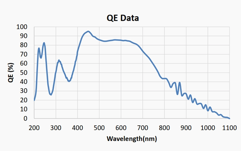
| QE | 95%@450nm |
| Conversion Range | 1x – 75x (HCG),1x – 50x (LCG) |
| Conversion Gain | 0.26e-/DN(High Sensitivity) 0.21e-/DN (HDR) |
| Dynamic Range | 62.1dB(High Sensitivity) 86dB(HDR) |
| Readout Noise | 0.74e-(High Sensitivity) 0.72e-(HDR) |
| Full Well Charge | 1.03ke-(High Sensitivity) 13.48ke-(HDR) |
| Maximum SNR | 30.1dB(High Sensitivity) 41.3dB(HDR) |
| Dark current | ≤0.05e-/s/pix@-10℃ ,≤0.01e-/s/pix@-20℃ |
| Sensitivity | 9.2×10⁷e⁻/((W/m2)·s)@450nm |
| Exposure Time Range | 12µs-300s |
| Binning Mode | Software 2×2~8×8, Hardware FPGA 1×1,1×2,2×1,2×2 |
| Shutter Mode | Roller Shutter / Global Reset |
| Data interface | USB3.2 Gen 2×1/10Gige |
| Digital I/O | 1 channel of optically isolated input, 1 channel of optically isolated output, 2 channels of non-isolated input/output port |
| Data Format | 8 bit / 12 bit / 16 bit |
| Cooling Temperature | -20℃ Air-cooled/-35℃ Water-cooled(specified at ambient temperature of +20℃) |
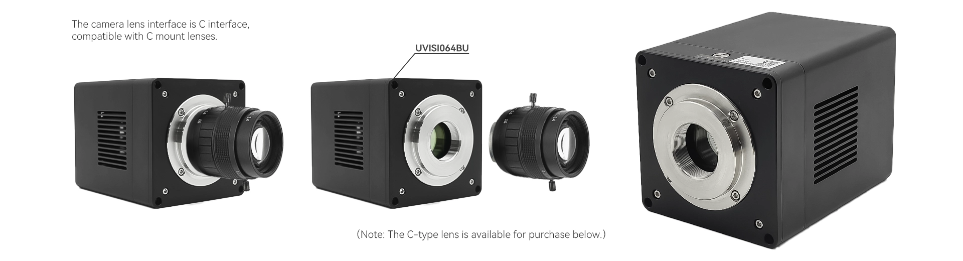
| Lens mount | C-mount |
| Power Supply | DC19V 4.74A |
| Power consumption | <46W@USB3.2 / <55W@10GigE |
| Size | 85×85×118mm |
| Weight | 976g |
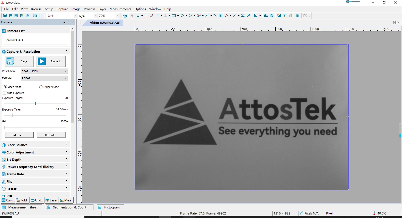
| Software | Complete SDK / AttosView |
| Operating Temperature | -30~60℃, |
| Storage Temperature | -40~85℃ |
| Humidity | 20%-80%,No condensation |
| Cerifcation | CE, FCC |
| Parameter | Specification |
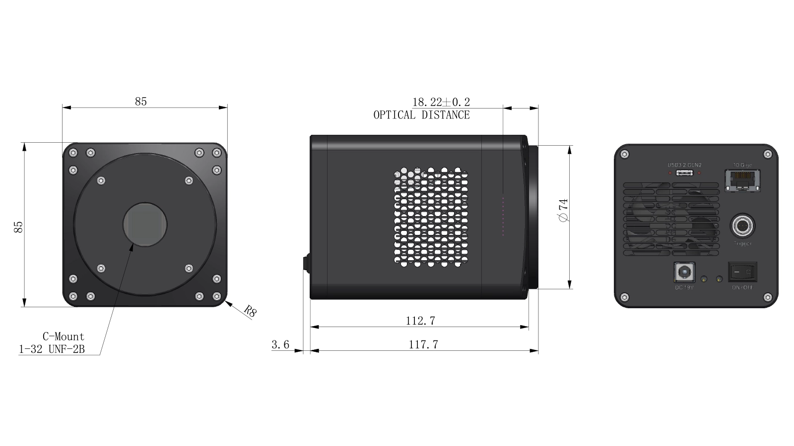
| Dimensions | 85mm×85mm×118mm |
| Lens Interface | C mount |
| Item | Specification |
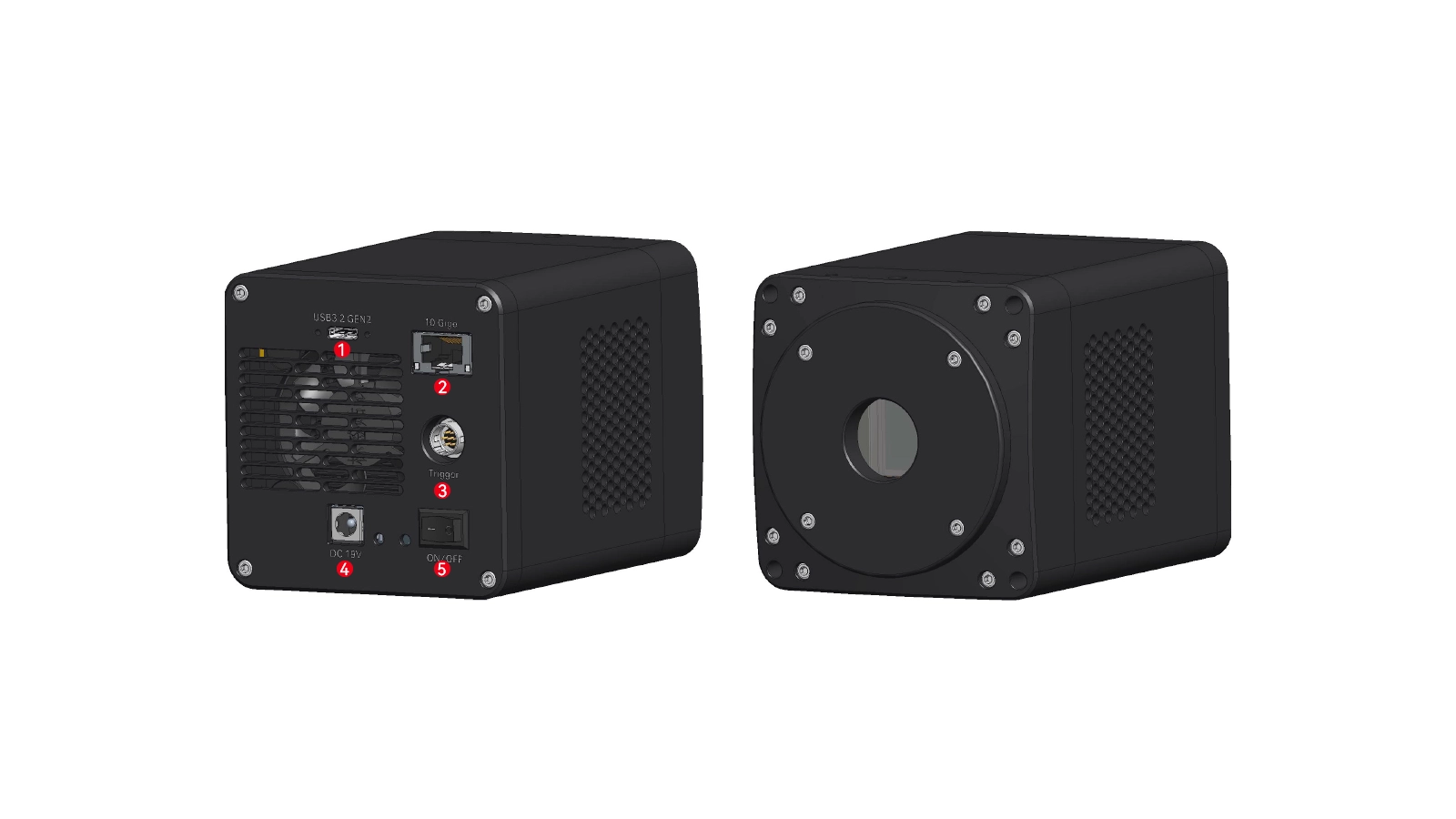
| 1 | USB3.2 GEN2Interface |
| 2 | 10 GigeInterface |
| 3 | ExternalIOInterface |
| 4 | DC 19V Power Connector |
| 5 | Power Switch |
| Table1: USB port, GigE port, CL port cooled camera pin signal definitions | |||||
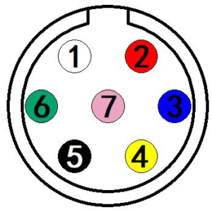 |
Color | Pin | Signal | Description of the signal | |
| White | 1 | GDN | Direct-coupled signal ground | ||
| Red | 2 | 12V | 12VDC power input | ||
| Blue | 3 | OPTO_GND | Opto-isolated signal ground | ||
| Yellow | 4 | DIR_GPIO0 | Direct-coupled General Purpose I/O (Software configurable input/output) (line2) | ||
| Black | 5 | DIR_GPIO1 | Direct-coupled General Purpose I/O (Software configurable input/output) (line3) | ||
| Green | 6 | OPTO_IN | Opto-isolated input signal (line0,input level 3.3~24V) | ||
| Pink | 7 | OPTO_OUT | Opto-isolated output signal (line1) | ||


The electrical characteristics of the opto-isolated output (external voltage 5V, external resistor 1K) are shown in Table 2.
| Table 2: Opto-isolated output signal’s electrical characteristics | ||
| Parameter name | Parameter notation | Parameter value |
| Output logic low | VL | 742mV |
| Output logic high | VH | 4.134V |
| Output rise time | TR | 4us |
| Output fall time | TF | 1.8us |
| Output rise delay | TDR | 12us |
| Output fall delay | TDF | 2us |
The output of the corresponding output current and VL when using different voltages and resistors in externalcircuit are shown in Table 3.
| Table 3:Opto-isolated output logic’s low levels parameters | |||
| External voltage | External resistor | VL | Output current |
| 3.3V | 1KΩ | 510mV | 2.82mA |
| 5V | 1KΩ | 742mV | 4.31mA |
| 12V | 2.4KΩ | 795mV | 4.68mA |
| 24V | 4.7KΩ | 850mV | 4.97mA |
1. Line2/line3 is set as input pin
Logic 0 input level: 0~0.6VDC (DIR_GPIO0/DIR_GPIO1 pins)
Logic 1 input level: 2.0~24VDC (DIR_GPIO0/DIR_GPIO1 pins)
Maximum input current: 25mA
When the input level is between 0.6V and 2.0V, the circuit action state is uncertain, please avoid the input voltage range working in this range.
To prevent damage to the GPIO pins, please connect the pin GND first, and then input voltage to the Line2 pin.
Input rise delay (TDR): 0.02us
Input fall delay (TDF): 0.02us
2. Line2/line3 are set as output pins
The maximum current allowed through this pin is 25mA.
The external pull-up voltage is 5V, the pull-up resistor is 1KΩ, and the GPIO is configured to output the logic level and electrical characteristics as shown in Figure 4.


When the ambient temperature is 25 degrees Celsius, the relationship between the external voltage, resistance and low-level voltage output is shown in Table 4.
| Table 4:Non-isolated output Logic’s low level parameters | ||
| External voltage | External resistor | VL(GPIO) |
| 3.3V | 1KΩ | 0.11V |
| 5V | 1KΩ | 0.167V |
| 12V | 2.4KΩ | 0.184V |
| 24V | 4.7KΩ | 0.385V |
| Table 5: Non-isolated output electrical characteristics | ||
| Parameter name | Parameter notation | Parameter value |
| Output rise time | TR | 0.08us |
| output fall time | TF | 0.02us |
| Output rise delay | TDR | 0.1us |
| Output fall delay | TDF | 0.04u |
ascamsdk support a variety of APIs, including: Native C/C++,.NET/C#/VB.NET, Python, Java, DirectShow, Twain, LabView, Matlab, etc. Compared with other APIs, Native C/C++ API as a low-level API is characterized by using pure C/C++ development without relying on other runtime libraries. The interface is simple and the control is flexible.
AttosTek provides extensive third-party software support for its UV-Vis cameras and SWIR cameras, facilitating rapid integration and use in various development environments. This includes SDK and demo programs for LabVIEW and MATLAB, as well as DirectShow drivers, Micromanager, and TWAIN SDK drivers. These features enable seamless compatibility with mainstream development environments and third-party software, greatly simplifying the workflow for system integration and secondary development.
|
AttosView Recommended System Requirements |
|
|
Operating System |
Microsoft® Windows® XP / Vista / 7 / 8 /10 /11(32 & 64 bit), Mac OSX, Linux |
|
Processor (CPU) |
≥3.0 GHz Intel Core i5 or Higher |
|
Memory (RAM) |
≥8 GB |
|
Hard Drive |
NVMe Solid State Drive (SSD) |
|
Graphics Card |
Dedicated Adapter with ≥256 MB RAM |
|
Motherboard |
USB 3.0 (-USB) Cameras: Integrated Intel USB 3.0 Controller or One Unused One Unused PCle3.0*16 Slot |
|
Connectivity |
Internet Connectivity for Driver Installation |
Q1 : What are the advantages of using this camera for low-light fluorescence imaging?
Q2: Why is this camera considered an all-rounder?
Q3:Why choose dual interfaces of USB3.2 and 10GigE for data?
The difference between a camera’s USB3.2 and 10GigE interfaces lies in their design goals: USB3.2 aims for high speed and easy connection over short distances, while 10GigE is designed for stable, high-bandwidth data transmission over long distances, with strong networking capabilities and support for long-distance operation.
Q4 :Why is the camera not showing up in the software?
Please first confirm that the camera’s data interface is properly connected, then check if the camera is in the computer’s Device Manager. If it is in Device Manager, it may be due to an incorrect software version and the software needs to be updated.
4MP, 6.5µm Pixel, High-Sensitivity sCMOS Scientific Camera
UVISI064BU10G
4 MP Back Illuminated sCMOS Camera, 6.5μm Pixels, 10GigE Interface
Optional accessories – lenses
AttosView offers an optional YLGD series continuous zoom optical system for visible light cameras, designed specifically for high-precision imaging scenarios. The YLGD series continuous zoom optical system series provides multiple focal length options and is suitable for various professional applications such as security surveillance, industrial vision inspection, and scientific observation, ensuring excellent image clarity, operational flexibility, and environmental adaptability. For inquiries, please contact sales@attostek.com .