Quantum efficiency (QE) is the probability that a single photon striking an image sensor produces a photoelectron that reaches the readout. A QE of 80% means eight photons out of ten are converted into signal; the other two are reflected or absorbed without charge. In scientific cameras, QE decides how much light a measurement needs, how long the exposure runs, and how clean the weakest signals look. Back-illuminated sCMOS and CCD sensors now reach 90% or more at their peak wavelengths, while many front-illuminated CMOS sensors stay near 60–70%. The rule is simple: match the QE curve to your emission wavelength, not just to the peak number on the datasheet.
Key Takeaways
- QE is a probability, not a sensitivity rating. It states the fraction of incident photons converted into photoelectrons, so 95% QE means 19 of 20 photons become signal and one is lost.
- Back-illuminated sensors beat front-illuminated designs by 20–30 points in peak quantum efficiency because light skips the wiring layers, which is why BSI sCMOS and CCD sensors dominate low-light imaging.
- External QE is the number that matters; internal QE ignores surface reflections and absorption losses, so it always looks higher than what the camera actually delivers at the focal plane.
- High QE alone does not make a good scientific camera. When fewer than a few hundred photons arrive per pixel, read noise and dark current decide image quality, not conversion efficiency.
- Match QE to the emission band, not the peak. A 95% peak at 450 nm serves fluorescence microscopy well, while a red-optimized curve is wasted if your label emits near 650 nm.
What Is Quantum Efficiency?
Quantum efficiency is the ratio between the number of photoelectrons collected and the number of photons that hit the detector. Every image sensor works the same way at the microscopic level: a photon arrives, its energy is absorbed in the semiconductor, and that energy promotes an electron into the conduction band. That mobile electron is the photoelectron, and photon detection in scientific cameras is essentially a counting game — count enough photoelectrons and the image is real; count too few and noise takes over.
Manufacturers quote two versions of the number. External QE is the honest one: photoelectrons divided by photons arriving at the sensor surface, including every photon lost to reflection and to absorption in coatings or wiring. Internal QE counts only photons that actually entered the semiconductor, so it ignores surface losses and always reads higher. When someone says a sensor has “95% quantum efficiency”, the number is almost always external QE measured at one wavelength, under controlled conditions. If the two values are shown separately, buy the external one — it predicts real image sensors in a real optical path.
Why Does Quantum Efficiency Matter in Scientific Cameras?
Scientific cameras exist to measure light that other cameras miss, and light sensitivity in these systems starts with quantum efficiency at the top of every signal chain. In a photon-limited measurement the signal-to-noise ratio grows with the square root of the number of detected photons, so doubling QE from 30% to 60% improves SNR by about 40% at the same exposure time. That extra margin is exactly what low-light imaging needs: shorter exposures freeze motion, lower illumination protects live samples, and dimmer fluorophores stay visible.
The practical example is fluorescence microscopy. A GFP-labelled sample emits only a few thousand photons per pixel per second, and each excitation cycle bleaches the dye a little more. A high-QE scientific camera lets the lab reduce laser power or exposure time without losing image quality, which directly extends how many frames a living sample survives. Photon detection that falls to 50% quietly doubles the exposure time your experiment needs. The same logic runs through astronomy, spectroscopy and photochemistry: QE is not a marketing number; it is a budget for how many photons your experiment can spend.
QE by Sensor Type
Three detector families dominate scientific cameras: CCD sensors, CMOS sensors and sCMOS technology. Their quantum efficiency differences come from how the pixel is built, not from the sensor material itself, which is almost always silicon in the 200–1100 nm range.
| Sensor architecture | Illumination design | Typical peak QE | Where it is used |
|---|---|---|---|
| CCD sensors | Front-illuminated | 50–65% | General spectroscopy, legacy systems |
| CCD sensors | Back-thinned | 90% and higher | Astronomy, single-molecule and photon-starved work |
| CMOS sensors | Front-illuminated with microlens | 60–80% | Machine vision, routine microscopy |
| CMOS / sCMOS technology | Back-illuminated (BSI) | 85–95% | Biomedical imaging, fluorescence microscopy, low-light scientific cameras |
Front-illuminated designs route light through the metal wiring and polysilicon gates on top of the pixel, so part of the signal is blocked before it reaches silicon. Back-thinned and back-illuminated (BSI) sensors remove that problem by etching the substrate thin and exposing the photoactive side directly to light; the wiring moves behind the photodiode. That single change lifts peak quantum efficiency by roughly 20–30 points and improves the blue and ultraviolet response most, because short wavelengths are absorbed very close to the surface. sCMOS technology took the CCD’s low-noise virtues and added CMOS speed and on-chip electronics, and BSI versions now reach peak QE figures that rival the best scientific CCDs. AttosTek’s high-sensitivity UV-VIS cameras cover 200–1100 nm with sCMOS, CMOS and CCD options, including a 4 MP 6.5 μm back-illuminated sCMOS camera rated at QE 95% at 450 nm. The same family adds spectroscopy CCD cameras for wavelength-resolved detection and 200–1100 nm CMOS camera models where format choice matters more than peak QE.
How to Read a Quantum Efficiency Curve
A quantum efficiency curve plots wavelength on the horizontal axis and QE on the vertical axis, and the shape of the line tells you more than the peak value. The curve rises from the ultraviolet end, reaches a plateau across the visible, and falls again toward the near-infrared as silicon stops absorbing light efficiently. Most image sensors share that silicon absorption physics, which is why their curves look similar in shape even when the peak heights differ.
Three features are worth checking. First, the peak position: a back-illuminated sensor typically peaks between 450 and 650 nm, where many fluorescence and astronomy signals live. Second, the fall-off toward 1000 nm — at 900–1000 nm the curve drops steeply unless the sensor uses deep-depletion silicon, which is why near-infrared work needs a different design. Third, the blue and ultraviolet end: short-wavelength photons are absorbed in the first tens of nanometres, so front-illuminated sensors lose most of the signal below 400 nm while BSI designs keep useful response down toward 200 nm with the right coatings. The datasheet value “QE 95% at 450 nm” describes one point; always compare the full curve against your light source and your emission band before choosing a camera.
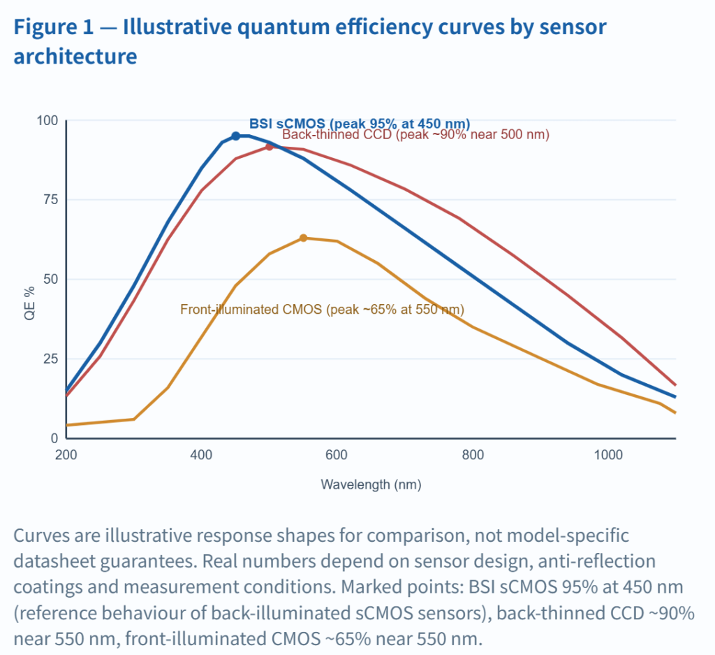
Figure 1 — Illustrative quantum efficiency curves by sensor architecture1007550250QE %2004006008001000Wavelength (nm)Front-illuminated CMOS (peak ~65% at 550 nm)Back-thinned CCD (peak ~90% near 500 nm)BSI sCMOS (peak 95% at 450 nm)
Curves are illustrative response shapes for comparison, not model-specific datasheet guarantees. Real numbers depend on sensor design, anti-reflection coatings and measurement conditions. Marked points: BSI sCMOS 95% at 450 nm (reference behaviour of back-illuminated sCMOS sensors), back-thinned CCD ~90% near 550 nm, front-illuminated CMOS ~65% near 550 nm.
Quantum Efficiency vs. Other Camera Specs
Quantum efficiency sets the ceiling on how many photons become electrons, but read noise, dark current, pixel size and full well set the floor below which those electrons cannot be seen. A camera with 95% QE and 8 e- read noise loses to a camera with 60% QE and 1 e- read noise when the signal is a handful of photons, because the noise term, not the conversion, limits the image. The SNR battle always runs on both sides of that equation.
As light levels rise, the balance shifts. At high signal levels read noise becomes irrelevant and QE plus full well decide dynamic range; at very short exposures read noise dominates again because there is little signal to average. That is why the specification sheet of a serious scientific camera lists QE together with read noise, dark current and dynamic range rather than alone. The flagship example in AttosTek’s UV-VIS line pairs QE 95% at 450 nm with 0.9 e- read noise and 83.4 dB dynamic range on a cooled back-illuminated sCMOS sensor, which is the combination that matters in practice — high conversion efficiency and low noise in the same pixel.
What Is a “Good” Quantum Efficiency?
There is no single threshold, but useful rules of thumb exist per application. For photon-starved science such as astronomy, single-molecule tracking and fluorescence microscopy, look for a peak QE of 90% or higher, preferably on a back-illuminated sensor, because every lost photon is lost data. For routine microscopy, machine vision and industrial inspection, a peak of 65–80% is normally enough — the extra 20 points of QE rarely justify the price gap. For ultraviolet work below 350 nm, a sensor holding 30–50% QE is already good, since surface absorption makes that band hard for any silicon detector.
Also check the QE at your working wavelengths, not only at the peak. Peak light sensitivity must sit inside your working band for the headline number to mean anything. A detector optimised for 450 nm will disappoint at 950 nm, so match the curve to the experiment: GFP and FITC emission around 510–530 nm, DAPI near 460 nm, red fluorophores near 650–700 nm, and NIR-II imaging beyond 1000 nm each need a different response profile. Light sensitivity in the real system also depends on optics and coatings, so a “good” sensor inside a mediocre optical path still produces dim images. If the target measurement sits in a specific narrow band, ask the vendor for the QE curve rather than the headline number.
To show how the numbers look on a real product, the table below lists the published highlights of AttosTek’s flagship back-illuminated sCMOS scientific camera, which combines high quantum efficiency with low read noise and a wide dynamic range in one cooled package.
| Parameter | Value |
|---|---|
| Sensor | GSENSE6504BSI back-illuminated sCMOS |
| Resolution | 2048 × 2048 |
| Pixel size | 6.5 μm |
| Peak quantum efficiency | 95% at 450 nm |
| Read noise | 0.9 e- |
| Dynamic range | 83.4 dB |
| Cooling | TEC to -25°C |
| Frame rate | Up to 270 fps at 8-bit |
| Interfaces | USB3.2 and 10GigE dual output |
| On-board memory | 4 Gb |
| Compliance | CE and FCC certified |
Conclusion
Quantum efficiency tells you how many of the photons you paid for actually become signal, and for scientific cameras it is the first specification to check. Understand the difference between external QE and internal QE, read the curve across the wavelengths you use, and weigh quantum efficiency against read noise, dark current and pixel design instead of chasing the highest peak number. Back-illuminated sCMOS sensors currently offer the best balance of QE, speed and low noise for most low-light imaging and fluorescence microscopy workloads. AttosTek covers the visible and ultraviolet range with cooled scientific cameras and interchangeable sCMOS, CMOS and CCD options, all 100% factory tested and CE/FCC certified, and every camera ships with AttosView control software and an SDK. If your experiment needs a specific spectral response, describe the target wavelengths to the AttosTek customization team for a configuration matched to your QE requirements.
FAQs
What is the highest quantum efficiency available in AttosTek’s scientific cameras?
The flagship UV-VIS sCMOS model, a 2048 × 2048 back-illuminated sensor with 6.5 μm pixels cooled to -25°C, is rated at QE 95% at 450 nm with 0.9 e- read noise and 83.4 dB dynamic range. It offers USB3.2 and 10GigE interfaces and reaches 270 fps at 8-bit, so the peak QE is available without sacrificing speed.
Can AttosTek customize the sensor or spectral response for a specific experiment?
Yes. Customization covers sensor type, resolution, pixel size and format, spectral response across EUV, visible, SWIR, MWIR and LWIR, plus frame rate, exposure, dynamic range and interfaces from USB3.0 and GigE to CoaXPress and CameraLink. Small-batch orders are accepted, so a single custom unit is a normal order rather than an exception.
What software and SDK support is included with the cameras?
Each camera ships with AttosView acquisition software and an SDK supporting C/C++, C#/VB.NET, Python and Java. Third-party environments including LabVIEW, MATLAB, Micro-Manager, DirectShow and TWAIN are also supported, so existing acquisition code usually carries over without a rewrite when a lab upgrades its detector.
Do CIF quotations include import duties and VAT?
No. A CIF quotation covers product cost, insurance and freight to the destination airport, but excludes destination-country duty, import tax, VAT and local charges. Logistics is a flat 50 USD per order within Asia and 100 USD elsewhere, quotations are issued in CNY, USD or EUR, and shipment goes by DHL or FedEx.
Are the cameras tested and certified before delivery?
Every AttosTek camera is 100% factory tested before shipment and carries CE and FCC certification. The team provides 7×24 expert support for integration, calibration and troubleshooting after delivery, and detailed datasheets including the QE curve are available for each sensor family before you order.