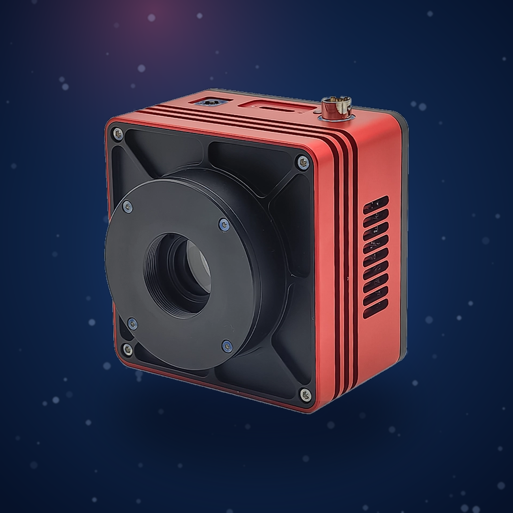
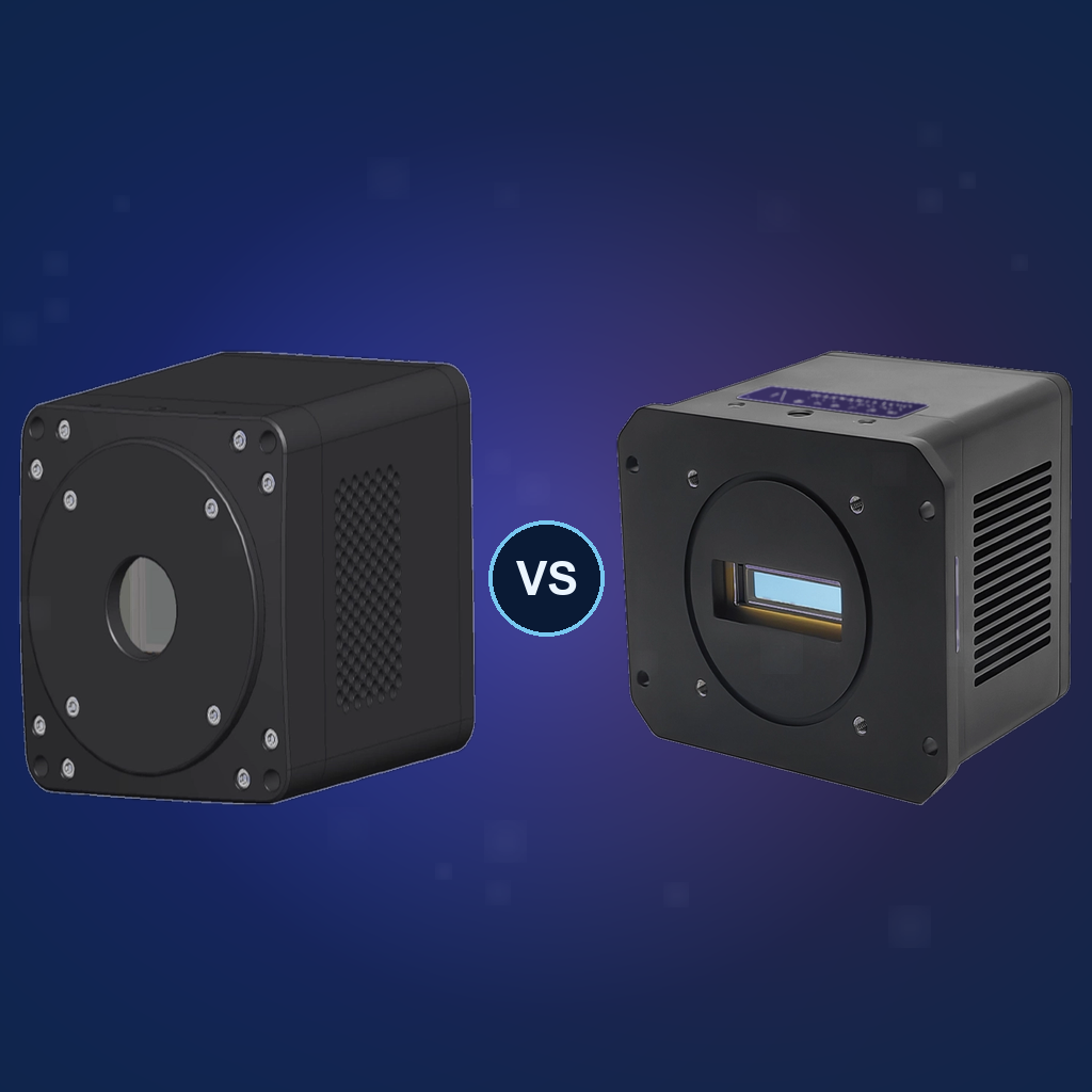
A SWIR camera images short-wave infrared — roughly 900–1700 nm — using an InGaAs focal plane array instead of silicon. Photons reflected by the target enter the lens, excite electrons in the indium gallium arsenide layer, and a readout integrated circuit (ROIC) bonded under every pixel converts that charge into a digital image. The result looks like a sharp black-and-white photograph, yet it reveals what visible and thermal cameras miss: silicon turns transparent, moisture turns dark and haze loses its grip. AttosTek builds cameras from 400 to 2700 nm with formats from 0.33 to 5 MP, in cooled and uncooled versions.
Key Takeaways
- Reflected light, not heat. The camera records photons in the 900–1700 nm short-wave infrared band, so images look like visible photos while silicon, smoke and haze lose their hiding power.
- InGaAs is the secret. Silicon stops absorbing above about 1100 nm, so SWIR uses an indium gallium arsenide focal plane array, hybridised pixel-by-pixel to a silicon ROIC.
- Wavelength reveals material. Silicon turns clear near 1150 nm and water absorbs strongly at 1450 nm, which is why semiconductor inspection and moisture detection are SWIR signatures.
- One band, many jobs. The same camera serves machine vision, non-destructive testing and night imaging without the heavy illumination power that a visible-light system would need.
- Formats from 0.33 to 5 MP, cooling to -80°C. AttosTek’s A-, B- and C-Series plus uncooled CQD designs cover 400–2700 nm for nearly every budget and workload.
How do SWIR Cameras Work?
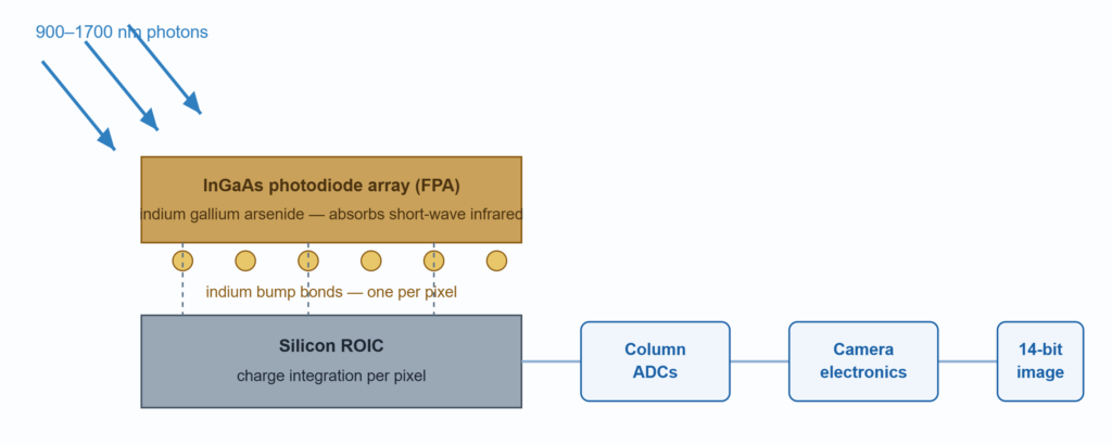
A SWIR camera is a three-stage photon pipeline. Stage one is optics: the lens focuses short-wave infrared light reflected by the target onto the focal plane array, the sensor chip at the back of the camera. Stage two is detection. The FPA is a two-dimensional grid of InGaAs photodiodes, a compound semiconductor whose bandgap lets it absorb photons with wavelengths far beyond what silicon can see. Each arriving photon in the 900–1700 nm window excites an electron-hole pair, and the photodiode collects those charges as a tiny current during the exposure.
Stage three is readout. Every photodiode pixel sits on top of a matching pixel in a silicon readout integrated circuit, the ROIC, and the two layers are connected through indium bump bonds one per pixel. During exposure the ROIC integrates the photocurrent into a charge packet; at the end of the exposure, column-parallel amplifiers and converters digitise the whole array at once and hand a 14-bit image to the camera electronics. Structurally this is close to a silicon CMOS sensor — same ROIC idea, same column readout — with the photodiode layer swapped to indium gallium arsenide to shift the wavelength response. Cooling the array suppresses dark current, which is why deep-cooled versions exist for the faintest signals.
Advantages of SWIR Cameras
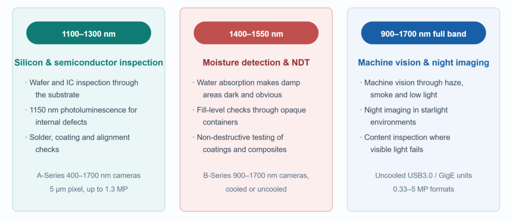
The first advantage is seeing through things. Silicon wafers and chips become transparent above about 1100 nm, so semiconductor inspection can look underneath the surface: 1150 nm emission imaging reveals internal wafer defects, and SWIR alignment cameras verify stack alignment through the substrate — silicon inspection in the most literal sense. Water absorbs strongly near 1450 nm, which turns moisture detection into a high-contrast measurement — damp patches, fill levels and wet coatings are immediately visible. Many plastics, adhesives and textiles also turn translucent in this band, which makes non-destructive testing practical: inspect the contents without opening, cutting or staining anything.
The second advantage is imaging in bad air and bad light. Short-wave infrared scatters far less than visible light in fog, haze and smoke, so the camera keeps rendering scenes that a visible system gives up on. Because the sensor reads reflected light, images stay familiar and sharp, and under starlight environments the sky itself provides enough signal for long exposures. Machine vision lines benefit directly: no glare saturation under bright lighting, no change in contrast when ambient light varies, and straightforward integration into existing machine vision frameworks built around a modern CMOS sensor, through standard USB3, GigE, CoaXPress or CameraLink interfaces. Compare the full line on the SWIR camera range.
New Imaging Technologies and SWIR Cameras
Traditional SWIR imaging was built around expensive, individually hybridised InGaAs focal plane arrays, which kept prices high and formats small. Three newer technologies are changing that. First, colloidal quantum dot (CQD) detectors: a thin quantum-dot layer is coated directly onto a silicon ROIC at low temperature, replacing the costly bump-bonded detector stack while covering 300–1700 nm uncooled. Second, extended-wavelength InGaAs: modified detector compositions push the response from 1700 nm out to 2200 nm and beyond for special material-identification tasks. Third, smaller pixels and wafer-level optics are raising resolution while cutting size and cost, bringing focal plane array designs closer to the economics of a consumer CMOS sensor.
State-of-the-art SWIR Cameras
Today’s high-end designs combine those threads. Resolution now reaches 5 MP at a 3.45 μm pixel pitch across 400–1700 nm, while deep-cooled B-Series models reach -50°C and -80°C for photon-starved fluorescence and laboratory work. Uncooled CQD cameras cover 300–1700 nm with no cooler at all, and extended C-Series sensors reach 1900–2700 nm. AttosTek’s portfolio mirrors this stack: the 1.3 MP 5 μm 400–1700 nm SWIR camera for high-resolution inspection, deep-cooled B-Series units for low-light research, and uncooled compact units on USB3.0 or GigE for production lines. Every unit ships CE/FCC certified and 100% factory tested.
| Technology | Wavelength | Cooling | Strength | Typical use |
|---|---|---|---|---|
| Hybrid InGaAs FPA | 900–1700 nm (400–1700 nm with extended response) | Cooled to -80°C | Highest sensitivity; mature formats from 0.33 to 5 MP | Semiconductor inspection, low-light science, night imaging |
| Extended InGaAs | 1900–2200 nm | Cooled to -50℃ | Wavelengths beyond the standard InGaAs cutoff | Material identification, special moisture and chemistry bands |
| CQD on silicon ROIC | 300–1700 nm | Cooled to -20℃ | Low cost, visible-plus-SWIR response, compact | Machine vision, OEM integration, education |
SWIR imaging solutions
SWIR earns its keep as part of a solution, not as a standalone sensor. On production lines it runs as a machine vision station for semiconductor inspection, silicon inspection and solder checks and same-colour sorting, tasks where the 900–1700 nm response finds contrast that visible cameras cannot register. In laboratories it works as a non-destructive testing tool for moisture detection and mapping, fill-level verification and composition checks, replacing destructive sampling with an instantaneous image. In the field it serves night vision, fog-penetrating traffic monitoring and solar panel inspection under starlight environments.
AttosTek packages these jobs end to end. The SWIR modular microscopic system pairs the camera with matched tube lenses, objectives and 1200–1550 nm LED illumination for microscopy-scale inspection from 900–1700 nm. On the camera side, uncooled USB3.0 and GigE models cover 400–1700 nm for line integration, deep-cooled B-Series units handle research-grade low light, and every camera ships with AttosView software plus an SDK for C/C++, C#/VB.NET, Python and Java. All products cover wavelengths from 1 to 14,000 nm across the range, are 100% factory tested and CE/FCC certified, and small-batch customization is welcome: describe your target and wavelength to the AttosTek customization team for a configuration and a CIF quotation.
Frequently Asked Questions
Which wavelength should I choose for my SWIR application?
Start from the material effect you need. Silicon and semiconductor inspection works around 1100–1300 nm where silicon is transparent, moisture detection concentrates near the 1450 nm water absorption band, and general machine vision covers the full 900–1700 nm window. If you need wavelengths beyond 1700 nm, extended InGaAs C-Series sensors reach 1900–2200 nm.
Do SWIR cameras always need cooling?
No. Uncooled InGaAs and CQD cameras are the standard choice for production lines and outdoor use, and AttosTek offers uncooled USB3.0 and GigE models from 0.33 to 5 MP. Deep cooling to -50°C or -80°C is reserved for photon-starved work such as fluorescence and NIR-II imaging, where every dark-current electron would otherwise bury the signal.
InGaAs or CQD — which detector technology should I pick?
InGaAs focal plane arrays deliver the highest sensitivity and the deepest cooling options, which suits scientific and low-light work. CQD (colloidal quantum dot) sensors coat directly onto a silicon ROIC, cutting cost while covering 300–1700 nm uncooled, which suits industrial and OEM budgets. Both ship with the same AttosView software and SDK support.
What interfaces and software come with AttosTek SWIR cameras?
Interfaces include USB3.0, GigE, CoaXPress, CameraLink and MIPI depending on the model. Every camera ships with AttosView acquisition software and an SDK supporting C/C++, C#/VB.NET, Python and Java, plus compatibility with LabVIEW, MATLAB, Micro-Manager, DirectShow and TWAIN, so existing machine-vision code usually carries over without a rewrite.
How do I get a quotation and how are the cameras shipped?
Send your target wavelengths, resolution and interface requirements, and AttosTek returns a configuration with a CIF quotation covering freight and insurance but excluding destination duty, import tax and VAT. Logistics is a flat 50 USD within Asia and 100 USD elsewhere, and every unit is 100% factory tested with CE/FCC certification before dispatch by DHL or FedEx.